
Boundary Scan Technology can not only test the logical functions of chips or PCBs but also check for faults in the connections between IC (Integrated Circuit) and PCB (Printed Circuit Board). Therefore, it has become mainstream in the design for testability of digital systems. The IEEE established the relevant standard, IEEE 1149.1, in 1990, which is formally titled IEEE Standard for Test Access Port and Boundary-Scan Architecture.
PART.1
Basic Principles of JTAG Technology
The boundary scan method extends the scanning path to the board or system level. Similar to the scanning path method, all information exchanged with components based on boundary scan design is transmitted serially, allowing test instructions and related test data to be sent serially to the components, and the execution results of the test instructions to be read out serially from the components. To achieve this functionality, boundary scan technology includes a scan chain composed of boundary scan register units connected to the chip pins, allowing the boundary signals of the components to be controlled and observed using scanning test principles. This is the meaning of boundary scan.
The basic principle of boundary scan technology is to add a register at the input and output ends of the core logic circuit. These registers have the following characteristics:
(1) Each register can both input and output data;
(2) All registers can be connected to form a shift register.
By adding these registers, core logic testing and testing of the connections between ICs and PCBs are realized.
PART.2
Basic Structure of JTAG
The test access port and boundary scan structure defined by the IEEE 1149.1 standard are fully compatible. This structure includes all JTAG modules defined in the IEEE 1149.1 standard, including the Test Access Port (TAP) Controller module, Instruction Register (IR) module, and Data Register (DR) module. The structure and the control relationships between each module are roughly illustrated in the following figure:
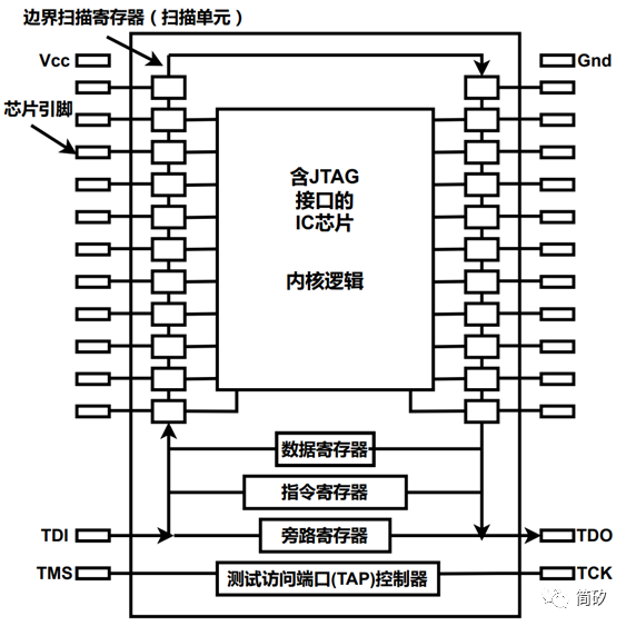
The TAP generates a set of control signals for the IR and DR based on the three input signals TRST (Test Reset), TCK (Test Clock), and TMS (Test Mode Select). It responds to the control sequences provided by the test access port and generates control sequences for the TAP (such as clock and control signals), thereby controlling other test modules. The IR module responds to the control from the TAP module to generate corresponding control signals, which then jointly control the actions of the DR module, such as moving data from TDI (Test Data Input) or TDO (Test Data Output).
PART.3
Introduction to JTAG Boundary Scan System Commands
The boundary scan logic is a logical system jointly controlled by the TAP Controller, DR, and IR. Therefore, commands occupy an extremely important position within the boundary scan logic system, as different commands constrain the different operations of the boundary scan logic. JTAG commands appear in binary encoded form, and the command width can be selected as needed. Command data is serially shifted into the instruction register from the TDI port on the rising edge of TCK when the TAP controller is in Shift-IR state.
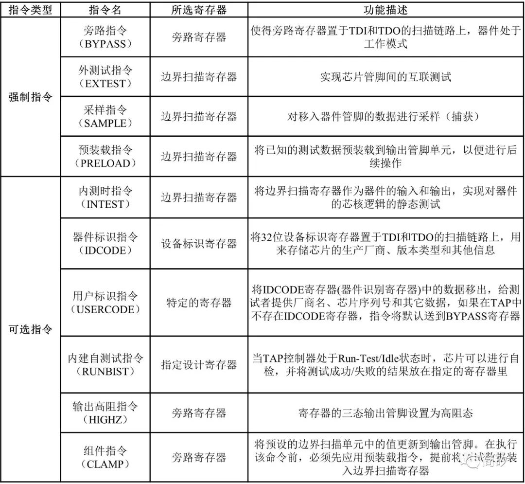
According to the IEEE 1149.1 standard, commands are classified into two categories. One category is public commands, which are universal for every boundary scan design; the other category is private commands, specifically designed by designers or manufacturers to complete particular test functions for dedicated data registers, and this type of command generally comes with detailed documentation from the designer or manufacturer. Public commands are further divided into two types: one is mandatory commands, as specified by the IEEE 1149.1 standard, and the other is optional commands. For convenience in discussion and comparison, the test commands are listed in the table below:
3.1
Mandatory Commands
-
BYPASS Command
The BYPASS command is an all-1 command of 11… Its function is to select the data register of the IC (or PCB) as the BYPASS Register (BR), at which point the scan chain of the IC (or PCB) consists solely of the 1-bit BR. The BYPASS command scans data from TDI to TDO through the 1-bit bypass register instead of through the entire boundary scan chain. This bypasses chips that do not need testing and shortens test time.
The reason for using all-1 data as the bypass command is to ensure that if the TDI of the IC experiences an open circuit fault, the bypass register is selected automatically to avoid unnecessary impacts from some unexpected events on the testing or operation of other ICs.
There are two methods to enable the bypass register: one is to maintain TDI at high level and complete an instruction scan cycle to enter the BYPASS command, and the other is to use the Device Identification Command (IDCODE) to select the bypass register. If the end of the data register is 0, or if there is no device identification register in the chip, the BR is selected automatically.
-
EXTEST Command
The EXTEST command is mainly used to test the connections between ICs (or PCBs) or the logic circuits outside the boundary scan design. It locks the data in the Boundary Scan Register (BSR) into the data register to stimulate the tested connections or external logic circuits, while this register captures the responses of the tested connections or external logic circuits under that stimulus. To complete the entire external test process, pre-load instructions should be applied to load the stimulus vectors into the BSR before executing the external test command. After completing the external test command, shift instructions should be used to shift the test results out for inspection.
-
SAMPLE/PRELOAD Command
The SAMPLE command is used to capture the signals at relevant sampling points (i.e., parallel input terminals in the boundary scan design) into the boundary scan register without affecting the normal operation of the core logic, for monitoring and analyzing the working conditions of the core logic circuit.
PRELOAD Command serves the same logical function as the SAMPLE Command, but the data loaded into the boundary scan register is known or predetermined by the operator. For example, during a certain test, a specific data can be preloaded to ensure that the boundary scan register outputs a completely safe state.
3.2
Optional Commands
-
INTEST Command
The INTEST command is used to test the core logic circuit. Its execution process is quite similar to that of the EXTEST command; however, due to the opposite positions of the tested objects, its stimulus and response terminals are also opposite. The INTEST command can isolate and test the internal circuits of each component on the circuit board.
Since the stimulus vectors are typically input serially when performing internal tests using boundary scan design, the testing speed is very low, only allowing for low-speed testing of the core logic, approximating static testing.
-
RUNBIST Command
This command provides a testing method for chip purchasers: to run the self-test functionality inside the device under a single command. This allows all devices providing the RUNBIST command on the board level to perform their self-test operations collectively, providing a quick and good condition check for the assembled PCB, meaning the chip has a self-check function. It does not require complex data and operations; executing the RUNBIST command allows for comprehensive self-testing of the chip’s internal logic. Unlike INTEST, it does not require additional test vectors. After self-testing is completed, data capture instructions should be used to load the self-test results into the boundary scan register, followed by shift instructions to serially shift the test results out at TDO for inspection.
-
CLAMP Command
When the CLAMP command is applied, the state of all signals driven out from the system output pins is entirely determined by the data stored in the BSR. Before loading this command, the content of the BSR can be preset using SAMPLE/PRELOAD commands. Under the CLAMP command, data is passed from TDI to TDO through the BYPASS register, without affecting the IC’s output.
-
Device Identification Register Command
When the IDCODE command is selected, the IC is in normal operating mode, connecting the Device Identification Register to TDI and TDO. The device identification register is a 32-bit register containing information such as the manufacturer, chip type, and version of the IC.
Since the IDCODE command is optional and not every chip has it, when executing the IDCODE command on a boundary scan chain to output all IDCODEs, chips with the IDCODE command will select the IDCODE register to output IDCODEs, while chips without the IDCODE command will automatically select the BYPASS register to output a “0”.
The USERCODE command allows users to program identification codes. This code contains unique programming information for external programmable devices (such as fuse programmable logic devices, FPGA, and CPLD). The circuit should provide a 32-bit user register to store user information (e.g., logic version or function information).
-
HIGHZ Command
This command can make all output terminals of the IC present a high impedance state, i.e., inactive state. It can be used during both non-boundary scan tests and boundary scan tests, mainly to prevent the output terminals from affecting other circuits and to protect the circuit.
Recruitment is ongoing
Address: Room 202, Building A9, Phase II, Software New City R&D Base, Tian Gu 8th Road, High-tech Zone, Xi’an, Shaanxi Province
Resume Submission Email: [email protected]
For more details, click here
Welcome to join and recommend!

✦
✦ ✦

WeChat ID | Jianxi Technology
Scan to Follow
Previous Issues Review