Debugging chips relies heavily on the JTAG interface. Downloading and debugging programs must be accomplished through the JTAG interface. Today, I learned some basic principles and working processes of the JTAG interface, and I will summarize them briefly.
The JTAG interface is an international standard testing protocol, originally initiated by several electronic device manufacturers who formed a Joint Test Action Group to establish standards for IC testing, which later became part of IEEE standards. The main use of JTAG is for online programming and debugging of systems.
The JTAG protocol includes four basic lines: TCK, TMS, TDI, and TDO, as well as extended signals like TRESET. TCK is the clock line, TMS is used for mode selection, TDI is data input, and TDO is data output. TRST is the reset line; since devices can also be reset via commands, the reset line is not mandatory. Additionally, extended JTAG signals may include return clocks and other signals.
1. Boundary Scan
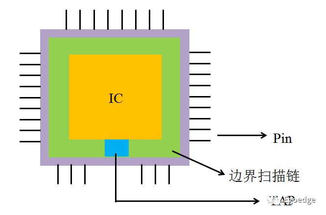
The working principle of JTAG is closely related to boundary scan technology. This technology involves adding a set of shift register units to each pin of the chip to monitor the state of each pin. These shift register units are known as boundary scan registers. All the shift registers within the chip can be connected together to form a boundary scan chain.
During chip debugging, the boundary scan registers isolate the chip from the external chip pins. For input pins, data can be written to the pins via the boundary scan registers; for output pins, the boundary scan registers can monitor the state of the pins. When the chip is functioning normally, the boundary scan registers are transparent to the IC and do not affect its operational state.
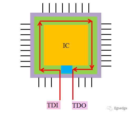
The boundary scan registers connect to form a boundary scan chain, allowing data from all pins of the chip to be serially input or output via TDI and TDO.
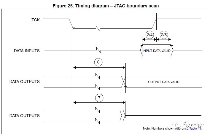
Through the boundary scan chain, signals output from and input to the IC can be monitored. Not only can data be written to the chip via the boundary scan chain, but signals can also be directly output to the chip’s pins. The signals stored in the boundary scan registers need to be input and output via TDI and TDO. Whether the signals are read or written, when the clock is active, the data shifts in the direction shown in the diagram below, completing the read and write operations serially.
2. Test Access Port (TAP)
With the boundary scan chain established, debugging also requires interaction with the boundary scan chain through the TAP interface. The TAP controller is used to control the TAP interface, enabling operations and access to the boundary scan chain.
The TAP controller can access all data registers (DR) and instruction registers (IR) of the chip. The operation of the chip and the composition of the program generally involve commands and data (addresses are also categorized as data here). Monitoring commands and data means monitoring the entire workflow of the chip. The debugging process can be understood as the PC accessing the chip’s instruction and command registers through the TAP interface.
When the TAP controller operates, the signals are driven by the rising edge of TCLK, with TMS signals switching the modes of the TAP interface, writing data to the chip via TDI, and reading data back through TDO.
The operations on data and instruction registers via the TAP interface primarily consist of 9 steps. After powering on, the sequence is Logic-Reset, Run-Test, Select-Scan, Capture-IR/DR (writing the logic sequence to the instruction or data register), Shift-IR (writing instructions to IR), Exit-IR/DR, Update-IR/DR, and finally returning to Run-Test mode. After one cycle, data from the data register can be captured or updates to the register data can be completed.
3. Emulator
Common development tools, such as Keil, IAR, and ADS, all have a common debugging interface called RDI, through which the PC sends data from the host to the target device. This process requires protocol conversion, transforming RDI data into JTAG data. There are two methods for this conversion: hardware-based and software-based.
Software-based conversion involves developing an application on the PC to convert RDI data into JTAG data, which is then sent out through the physical interface on the PC, with hardware devices converting the signal levels to match the IC interface levels. The principle of H-JTAG operates this way. The advantage is that the hardware is simple and only responsible for signal level conversion.
Hardware-based conversion sends RDI data through the physical interface of the PC, which is then converted to JTAG data by hardware. Typically, hardware-based solutions involve a CPU, commonly a microcontroller, to perform protocol conversion, such as J-LINK. Hardware-based solutions are faster due to the microcontroller performing the protocol conversion, but the hardware tends to be more complex.