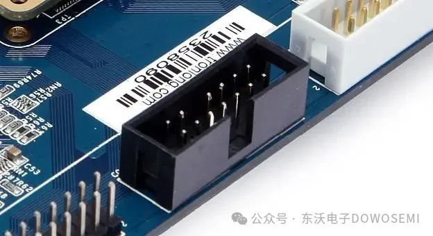
The JTAG interface is a type of interface used for downloading programs, and it is also frequently connected and disconnected while powered. It is well-known that hot-plugging can inevitably generate some surges or ESD (Electrostatic Discharge). Therefore, if protective measures are not taken, it is easy for surge ESD to break down the JTAG-related pins, potentially damaging the internal core components of the CPU, leading to permanent damage to the internal circuitry. To address the surge ESD issues of the JTAG interface, Dongwo Electronics has designed a protection scheme diagram and recommended corresponding protective components.
Dongwo JTAG Interface Surge ESD Protection Scheme Diagram (ESD Diode Edition)
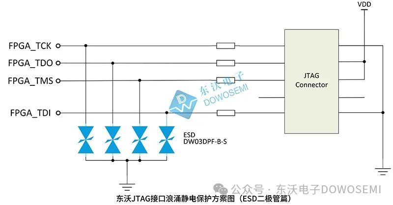
From the scheme diagram, it can be seen that Dongwo Electronics recommends using four ESD diodes DW03DPF-B-S to protect its interface. The Dongwo DW03DPF-B-S5 works at a voltage of 3.3V, with a clamping voltage of 9.4V, low leakage current of 0.5uA, and junction capacitance as low as 60pF. According to IEC 61000-4-2, it can provide ESD protection of up to ±30kV (air discharge) / ±30kV (contact discharge); according to IEC 61000-4-5, it can withstand a peak pulse current of 30A (8/20us) and a peak pulse power of 330W (8/20us), providing reliable static and surge protection for interface chips. The Dongwo DW03DPF-B-S is bidirectional and uses a DFN1006-2L small package, making PCB layout convenient.
Dongwo JTAG Interface Surge ESD Protection Scheme Diagram (Schottky Diode Edition)
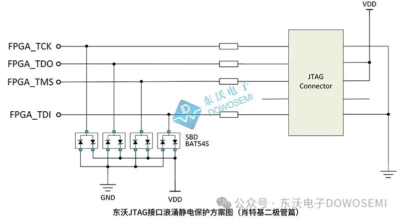
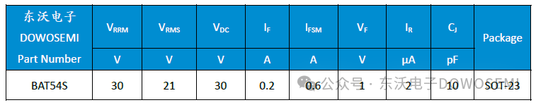
From the scheme diagram, it can be seen that Dongwo Electronics uses a clamping diode to protect the signal interface. The diode selected is the Schottky diode BAT54S, which has a reverse breakdown voltage of 30V, forward current of 0.2A, and a leakage current as low as 2uA. Under the chip’s 3.3V operating voltage, it can clamp the signal level to around ±4.1V, thus better protecting the interface chip from the effects of static electricity or surges.
JTAG Interface Surge ESD Protection Device Parameters
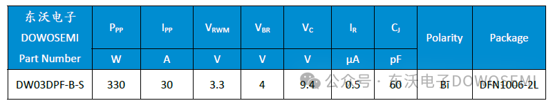
1) ESD Diode DW03DPF-B-S Parameters
Refer to the Dongwo Electronics “ESD-DW03DPF-B-S Datasheet” for detailed parameters as follows:
2) Schottky Diode BAT54S Parameters
Refer to the Dongwo Electronics “SBD-BAT54~BAT54S (SOT-23) Datasheet” for detailed parameters as follows:
The above is the classic protection scheme design diagram for Dongwo JTAG interface surge ESD. If you have special needs, feel free to discuss. For surge ESD protection schemes, choose Dongwo Electronics for reliable circuit protection!

Dongwo Recommended Solutions:
1) 1000M Ethernet POE Surge ESD Protection Circuit Diagram
2) Automotive EPS Module Load Dump Protection Circuit Design Diagram
3) Type-C Port Integrated ESD Surge Protection Scheme Design Diagram
4) USB PD Fast Charge Interface Surge ESD Protection Circuit Diagram
5) 24V System Overload Test Protection Circuit Diagram and TVS Device Selection Guide
6) USB3.0 High-Speed Interface ESD Surge Protection Scheme
7) HDMI High-Definition Multimedia Interface ESD Surge Protection, How to Select TVS Diodes?
8) Dongwo CAN Controller Local Area Network Bus Surge ESD Protection Scheme
9) RS-232 Interface Surge ESD Protection Circuit Diagram, Comprehensive
10) AC 220V Power Supply Interface Surge Protection Scheme and Protective Device Selection
Click below to follow Dongwo, reliable circuit protection!