Basic structure of JTAG:
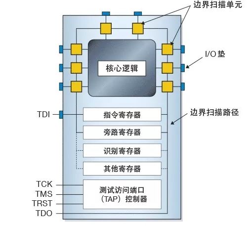
Standard Ports:
TCK (Test Clock) – This signal synchronizes the operation of the internal state machine.
TMS (Test Mode Select) – This signal samples at the rising edge of TCK to determine the next state.
TDI (Test Data Input) – This signal represents the data for the device under test or programming logic. It is sampled at the rising edge of TCK when the internal state machine is in the correct state.
TDO (Test Data Output) – This signal represents the data from the device under test or programming logic and is valid at the falling edge of TCK when the internal state machine is in the correct state.
TRST (Test Reset) – This is an optional pin that, when present, can reset the TAP controller’s state machine.
Registers:
The instruction register holds the current instruction. Its contents are used by the TAP controller to determine how to handle received signals. Typically, the contents of the instruction register define the signal passed to the data register.
Data registers: bypass register, identification register, and other data registers.
JTAG State Machine:
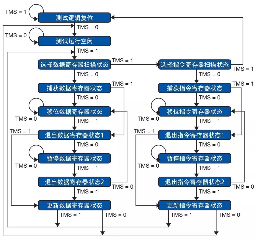
1. Reset state of the state machine. At the rising edge of TCK, if TMS is low, it transitions to the next state; otherwise, it remains unchanged.
2. Run-Test/Idle state. At the rising edge of TCK, if TMS is high, it will cause a state transition to the data channel communication state; otherwise, it remains unchanged.
3. Select-DR Scan state. In this state, reading a low TMS at the rising edge of TCK will enter the data channel; reading a high TMS will switch to the instruction channel.
4. Select-IR Scan state. In this state, reading a low TMS at the rising edge of TCK will enter the instruction channel; reading a high TMS will switch to the reset state.
1. Capture DR state. Capture data.
2. Shift DR state. The state for data transfer through TDI and TDO. During this period, keep TMS low, and when sending the last data, set TMS high, so that at the rising edge of TCK, the system completes the transfer of the last data and successfully exits the Shift DR state.
3. Exit1 DR state. At the rising edge of TCK, if TMS is high, it enters the Update-DR state.
4. Update-DR state. The contents of the shift register are read in parallel into the corresponding registers.
The JTAG instruction set includes the following common instructions:
EXTEST Instruction
External test instruction, must be all 0, defined by TAP. This instruction initializes external circuit testing, mainly used for board-level interconnect and off-chip circuit testing.
EXTEST instruction connects the scan register BSR between TDI and TDO in the Shift-DR state. In the Capture-DR state, the EXTEST instruction loads the state of input pins into BSR at the rising edge of TCK. The EXTEST instruction never uses the data in the input latches loaded into BSR, but captures data directly from the pins. In the Update-DR state, the EXTEST instruction drives the data in the parallel output register unit to the corresponding output pins at the falling edge of TCK.
SAMPLE/PRELOAD Instruction
Sample/Preload instruction, defined by TAP. In the Capture-DR state, the SAMPLE/PRELOAD instruction provides a snapshot of the data flow from the pins to the on-chip system logic, captured at the rising edge of TCK. In the Update-DR state, the SAMPLE/PRELOAD instruction latches the data in the BSR register unit to the parallel output register unit, and then the EXTEST instruction drives the latched data in the parallel output register unit to the corresponding output pins at the falling edge of TCK.
BYPASS Instruction
Bypass instruction, must be all 1, defined by TAP. The BYPASS instruction places a 1-bit bypass register between TDI and TDO, allowing the shift operation to go through only a 1-bit bypass register instead of many bits (equivalent to the number of pins) of boundary scan register BSR, thus improving efficiency when testing other chips connected on the same JTAG chain outside the main CPU.
IDCODE Instruction
Read CPU ID instruction, defined by TAP. This instruction connects the processor’s ID number register between TDI and TDO.
INTEST
This instruction connects TDI and TDO lines using a boundary scan register (BSR). The EXTEST instruction allows users to set and read pin states, while the INTEST instruction is associated with the device’s core logic signals.
IJTAG: INTERNAL JTAG
Fully compatible with JTAG network
Describes the network structure between TDR to TDR
SIB flexibly configures TDR
Specifies the interaction language between TDR and IP
Plug and play
Network connection language: ICL
Program description language: PDL
Concept of SIB:
Segment-Insertion-Bit, has on and off states
Through the TAP controller, TDI input TDR can control the on and off of SIB, thus controlling the corresponding IP.