Skip to content
Source: FPGA Resource Hero
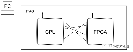
In the process of FPGA development and learning, a critical step is the board download implementation. Achieving hardware “hard realization” is crucial, and generally, the JTAG interface is more commonly used. Therefore, many experts must have encountered issues with the JTAG interface malfunctioning or being damaged and unusable. Recently, I faced such a situation where the JTAG interface of my FPGA suddenly could not download programs anymore, and this was not the first time it happened. During previous projects, I also encountered similar issues, where it worked well one day and then failed the next, which was quite frustrating. As a result, I tried many solutions; initially, I did not consider that the JTAG interface was damaged. So, I replaced the USB Blaster, but there was no response at all. Could it really be that the JTAG interface was broken? Thus, I referred to relevant materials to understand the essence of the problem. Below are some of my findings, shared for your reference, hoping to engage in mutual learning.
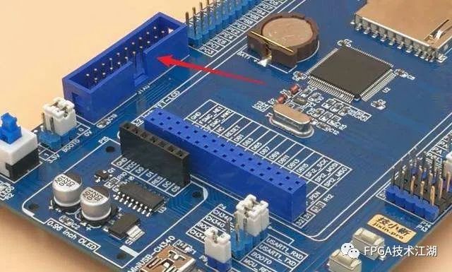 Based on the materials I reviewed and my practical experience, during the use of the JTAG download interface, please do not randomly plug and unplug it while powered on, as this can damage the signal pins of the FPGA chip’s JTAG interface. How can you confirm if the JTAG interface is damaged? First, you need to rule out some basic factors: 1) whether the connections are matched. Many devices correspond to many interfaces, and under actual conditions, they need to be matched correctly; otherwise, similar issues may arise. 2) Rule out problems with the download cable. If the download cable is faulty, you can try multiple download cables to eliminate this issue. If you still cannot access the FPGA’s JTAG interface, it is very likely that the JTAG interface of your FPGA chip is damaged. At this point, please use a multimeter to check if TCK, TMS, TDO, and TDI are short-circuited to GND. If any signal is short-circuited to ground, it indicates that the JTAG signal pin is damaged.
As for what JTAG is, let’s discuss it here. JTAG stands for Joint Test Action Group.
JTAG is an IEEE standard used to solve board-level issues, born in the 1980s. Today, JTAG is used for programming, debugging, and probing ports. Of course, its original use was boundary testing.
For example, if you have two chips connected by many wires, how can you ensure that these wires are connected correctly? Using JTAG, it can control all IC pins. This is called chip boundary testing.
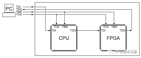
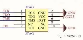
JTAG has developed to now have pins, typically four: TDI, TDO, TMS, TCK, and there is also a reset pin TRST. The JTAG pins on the chip are actually dedicated.
Based on the materials I reviewed and my practical experience, during the use of the JTAG download interface, please do not randomly plug and unplug it while powered on, as this can damage the signal pins of the FPGA chip’s JTAG interface. How can you confirm if the JTAG interface is damaged? First, you need to rule out some basic factors: 1) whether the connections are matched. Many devices correspond to many interfaces, and under actual conditions, they need to be matched correctly; otherwise, similar issues may arise. 2) Rule out problems with the download cable. If the download cable is faulty, you can try multiple download cables to eliminate this issue. If you still cannot access the FPGA’s JTAG interface, it is very likely that the JTAG interface of your FPGA chip is damaged. At this point, please use a multimeter to check if TCK, TMS, TDO, and TDI are short-circuited to GND. If any signal is short-circuited to ground, it indicates that the JTAG signal pin is damaged.
As for what JTAG is, let’s discuss it here. JTAG stands for Joint Test Action Group.
JTAG is an IEEE standard used to solve board-level issues, born in the 1980s. Today, JTAG is used for programming, debugging, and probing ports. Of course, its original use was boundary testing.
For example, if you have two chips connected by many wires, how can you ensure that these wires are connected correctly? Using JTAG, it can control all IC pins. This is called chip boundary testing.
JTAG has developed to now have pins, typically four: TDI, TDO, TMS, TCK, and there is also a reset pin TRST. The JTAG pins on the chip are actually dedicated.
-
TDI: Test Data Input, data is input to the JTAG interface through TDI;
-
TDO: Test Data Output, data is output from the JTAG interface through TDO;
-
TMS: Test Mode Select, used to set the JTAG interface to a specific test mode;
-
-
CPU and FPGA manufacturers allow JTAG for port debugging; FPGA vendors allow configuration of FPGA through JTAG, using JTAG signals into the FPGA core.
The PC controls JTAG: Connect the JTAG cable to the PC’s printer port, USB, or network port. The simplest connection is to the printer port.
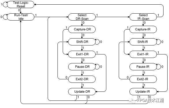
TMS: Inside each chip containing JTAG, there is a JTAG TAP controller. The TAP controller is a state machine with 16 states, and TMS is the control signal for this device. When TMS connects all the chips together, the TAP state transitions of all chips are consistent. Below is a schematic diagram of the TAP controller:
Changing the value of TMS will cause the state to transition. If a high level is maintained for 5 cycles, it will jump back to test-logic-reset, usually used to synchronize the TAP controller; the two most important states are Shift-DR and Shift-IR, both connecting TDI and TDO.
IR: Instruction Register, you can write values to this register to instruct JTAG to perform a task. Each TAP has only one IR register, and its length is fixed.
DR: The TAP can have multiple DR registers, similar to the IR register; each IR value selects a different DR register.
4. JTAG Chain Related Questions
Calculating the number of ICs in the JTAG chain:
An important application is when the IR value is all ones, representing the BYPASS command. In BYPASS mode, the DR register in the TAP controller is always single-bit, from input TDI to output TDO, usually one cycle, doing nothing.
You can use BYPASS mode to calculate the number of ICs. If the TDI-TDO chain delay of each IC is one clock, we can send some data and detect how long it is delayed, then we can deduce the number of ICs in the JTAG chain.
Obtaining the Device ID in the JTAG Chain:
Most JTAG ICs support the IDCODE command. In the IDCODE command, the DR register will load a 32-bit value representing the device ID. Unlike the BYPASS instruction, there is no standard IR value in IDCODE mode. However, each time the TAP controller transitions to the Test-Logic-Reset state, it enters IDCODE mode and loads the IDCODE into DR.
When the TAP controller enters boundary scan mode, the DR chain can traverse each IO block or read or intercept each pin. Using JTAG on an FPGA, you can know the status of each pin while the FPGA is running. You can use the JTAG command SAMPLE, of course, different ICs may vary.
 If the JTAG interface is damaged, then you can only “mourn the loss,” but do not just focus on the sorrow; the most important thing is to analyze the causes. This principle applies to other matters as well. Let’s analyze the situation: we may often plug and unplug the JTAG download port for convenience; in most cases, this will not cause problems. However, there is still a small chance of the following issues arising, due to electrostatic discharge and surges caused by hot swapping, ultimately leading to the breakdown of FPGA pins. Furthermore, some have suspected whether it is due to counterfeit USB Blasters or ByteBlasterIIs simplifying designs and removing protective circuits. However, after much feedback from practical situations, it has been proven that original USB Blasters can also experience the same issue. Others have questioned whether ALTERA’s low-end chips lack diode clamp protection circuits to reduce costs. Such doubts do not fundamentally address the problem; what is most important is to standardize operations and minimize premature termination of hardware devices and interfaces due to improper actual operations. Now, the key point is how we should standardize the operation of the JTAG download interface.
Power-On Operation Sequence:
If the JTAG interface is damaged, then you can only “mourn the loss,” but do not just focus on the sorrow; the most important thing is to analyze the causes. This principle applies to other matters as well. Let’s analyze the situation: we may often plug and unplug the JTAG download port for convenience; in most cases, this will not cause problems. However, there is still a small chance of the following issues arising, due to electrostatic discharge and surges caused by hot swapping, ultimately leading to the breakdown of FPGA pins. Furthermore, some have suspected whether it is due to counterfeit USB Blasters or ByteBlasterIIs simplifying designs and removing protective circuits. However, after much feedback from practical situations, it has been proven that original USB Blasters can also experience the same issue. Others have questioned whether ALTERA’s low-end chips lack diode clamp protection circuits to reduce costs. Such doubts do not fundamentally address the problem; what is most important is to standardize operations and minimize premature termination of hardware devices and interfaces due to improper actual operations. Now, the key point is how we should standardize the operation of the JTAG download interface.
Power-On Operation Sequence:
-
1. With the FPGA development board and related devices powered off, plug in the JTAG download cable;
-
2. Connect the USB Blaster or ByteBlasterII cable;
-
3. Power on the FPGA development board.
Power-Off Operation Sequence:
-
1. Disconnect the power of the FPGA development board and related devices;
-
2. Disconnect the USB Blaster or ByteBlasterII cable;
-
3. Unplug the JTAG download cable and store it in a suitable place.
Although the above operation steps may seem cumbersome, and sometimes we may overlook them during use, to ensure that the chip is not damaged, it is recommended that everyone follow these steps diligently. The issue I encountered above was due to TCK being short-circuited to GND. Although the probability of occurrence is not very high, to reasonably and sustainably use hardware-related devices, it is still advisable to operate in a standardized manner. From a different perspective, “practicing more” is also beneficial for oneself. Finally, I’d like to remind everyone that it is best not to hot-swap the JTAG download interface while powered on, which can at least prolong the lifespan of the JTAG interface. After all, a long-term relationship is quite nice; don’t wait until you lose it to regret it.
Working Principle of Computers: RAM Series – Eight-Bit Register
Working Principle of Computers: RAM Series – Flip-Flop
What is the most impressive analog circuit? What is clever about this circuit?
How to describe your job position to relatives when going home for the New Year? Hardware engineers can get confused explaining themselves
5 yuan turns into 70, oh no, there’s a chip shortage again
PCB design must be well thought out; the basic process is indispensable