
This article introduces four types of JTAG data registers, namely:
-
Boundary Scan Register (BSR) -
Bypass Register (BR) -
Device ID Register -
User Data Register(s)
Before discussing the boundary scan register, it’s important to first understand why we need a boundary scan register.
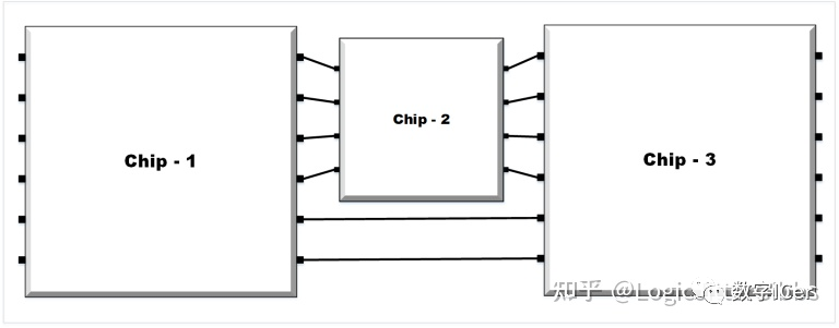
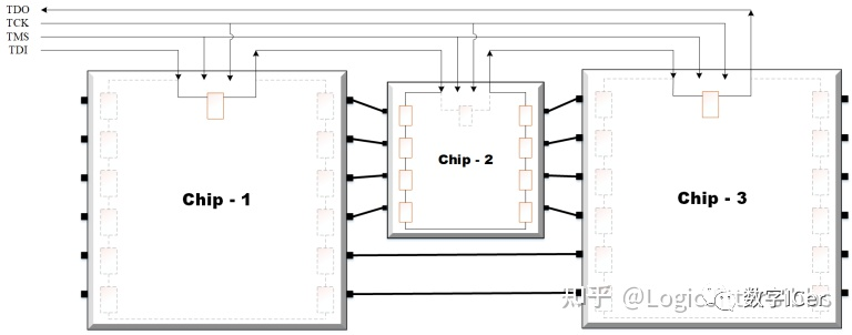
Assume a scenario where we need to solder and assemble three chips developed and produced by different manufacturers onto the same circuit board. These chips have all passed testing by their respective manufacturers using Automatic Test Equipment (ATE).
However, if connectivity issues arise after assembling them onto the circuit board, how can we detect the connection faults? If we only test for connectivity issues, we cannot send the circuit board back to ATE to retest all the chips, as ATE is very expensive.
In the example shown in Figure 1, the IO of Chip 2 is not board-level IO. If we want to access Chip 2 for some debugging reasons, how can we do that?
Boundary Scan Register (BSR)
The boundary scan register is designed to solve the two issues mentioned above.
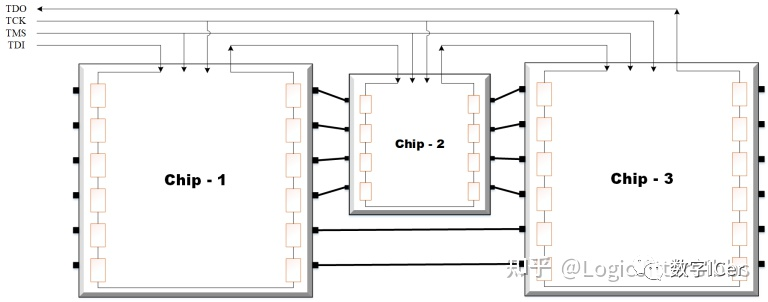
If all three chips support JTAG access and boundary scanning, we can control and observe the IO of any device, even if they are not board-level IO. Similar to the concepts of scanning and ATPG (Automatic Test Pattern Generation), we can shift the values we want into the BSR and observe the results in the BSR to test the connectivity between chips. This type of testing is referred to as boundary scan testing.
The JTAG interface allows multiple devices to connect to the same JTAG interface in a Daisy Chain manner. Specifically, TMS and TCK are connected in parallel to each device, while TDI and TDO are connected serially as shown in Figure 2.
Note: There can only be one TAP (Test Access Port) at any level in the system (board level/chip level/IP module level). Therefore, all chips use the same TAP instead of each chip having a dedicated TAP.
The registers in the Boundary Scan Register (BSR) are inserted between the device’s core logic and IO pins. In normal operating mode, these units are bypassed, effectively rendering them non-existent. In test mode, the BSR is enabled and can be used to control the IO pins and read the current values on the IO pins.
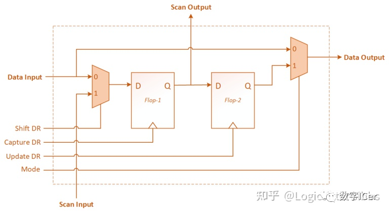
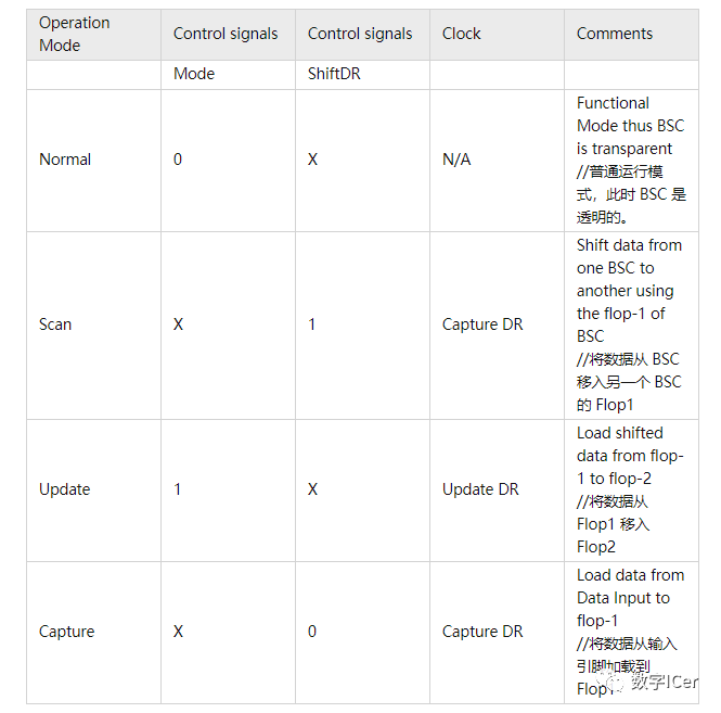
BSC supports four modes, each as shown in the table below.
Bypass Register (BR)
The bypass register is a 1-bit wide register that provides a direct path between TDI and TDO. The existence of this direct path can minimize testing time overhead for devices in the circuit. Assume we have multiple serially connected chips on the circuit board, as shown in Figure 4, and we want to access a single chip, such as Chip 2. In the traditional approach without a bypass register, we would need to shift data through all BSCs in Chip 1 and Chip 3 to access the BSC in Chip 2, which adds unnecessary shifting time overhead. To avoid this delay, we need to bypass all BSCs in Chip 1 and Chip 3, so that when data passes through JTAG devices like Chip 1/3, each JTAG device only incurs one clock cycle of delay.
In the above example, specifically:
If we go through Chip 1 and Chip 3, it would take 12 + 8 + 12 = 32 clocks.
However, if we bypass Chip 1 and Chip 3, it only takes 1 + 8 + 1 = 10 clocks.
When we need to bypass a chip, we need to load the opcode corresponding to the Bypass register into the instruction register, enabling the instruction decoder logic to establish a bypass TDI-TDO path that only passes through the Bypass register.
Device ID Register
The ID register is used solely for device identification. Assume we have multiple JTAG devices sharing a debug interface or TAP. To ensure we are accessing the correct debug interface, each device has an ID register, with a value (i.e., device ID code) that is unique. The device ID is used to help users or debugging tools identify and confirm they are accessing the correct debug interface.
User Data Register(s)
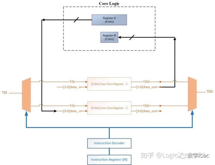
These user-defined registers are used to control or observe internal functional registers and internal ports in the core logic during debugging, as shown in Figure 5. Generally, the internal functional registers accessible via JTAG provide two sets of interfaces: one for JTAG access and one for normal functional logic access. You can refer to the JTAG access example in the next section to understand how we access internal functional logic registers through user data registers.
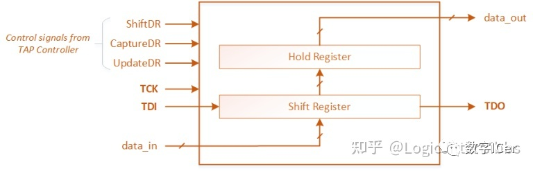
Similar to the instruction register, the user data register also includes two levels of registers, as shown in Figure 6. The Hold register retains previous data, while the Shift register gradually shifts in new data without affecting the current data. The control signals for the user data register come from the TAP controller, with the specific control signal values depending on the current FSM state, allowing the user data register’s Shift register to shift in/out user data (i.e., the serial update process in Shift-DR state) or to pass the contents of the Shift register to the Hold register (i.e., the parallel update process in Update-DR state).
It is worth noting that we can design multiple user data registers, each with a different opcode.Only after loading a specific opcode into the instruction register will the corresponding user data register become readable and writable, allowing control and observation of the corresponding internal functional logic.
Translated by: Zhihu LogicJitterGibbs Original link: https://link.zhihu.com/?target=https%3A//vlsitutorials.com/jtag-architecture-overview/

Previous Recommendations
SoC Design: Bus Interfaces
SoC Design: Low Power
Perl in IC Applications
EDA Tutorials
Chip Design
UVM Chip Verification
FPGA Series
Vivado Advanced
Formal Verification
Digital C Written Exam
Digital IC Interview Questions
Excellent IC/FPGA Open Source Projects
Synthesis and Timing Analysis
Disclaimer: Unauthorized reproduction is prohibited