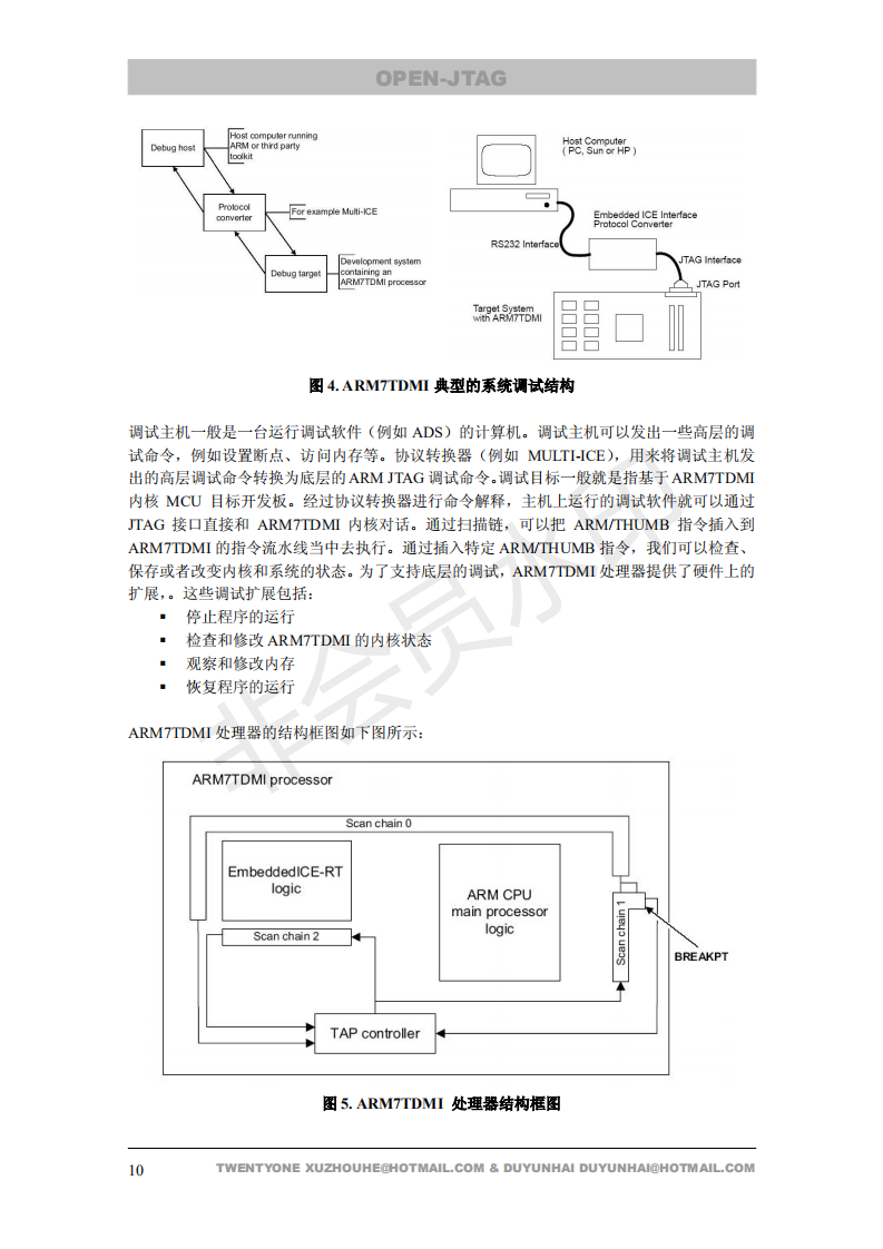
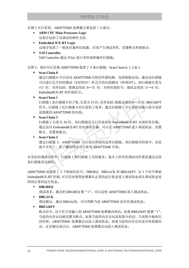
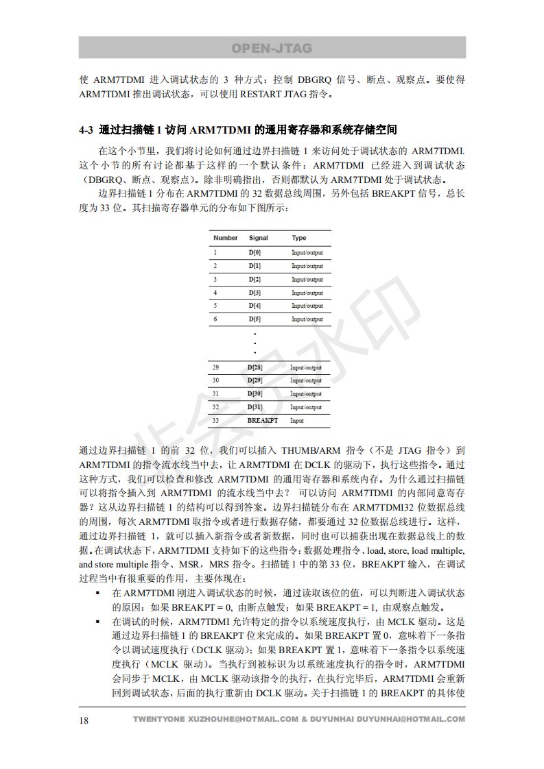
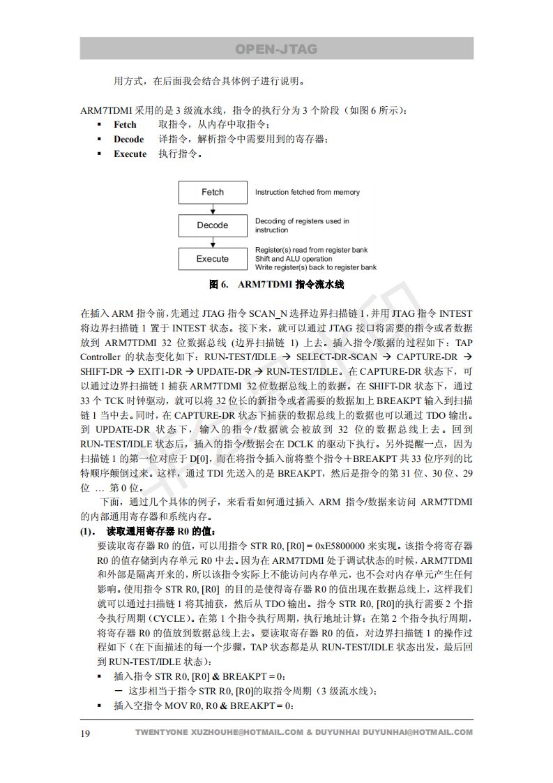
Introduction to JTAG
JTAG (Joint Test Action Group) is an international standard testing protocol (IEEE 1149.1 compliant), primarily used for internal testing of chips. Most advanced devices today support the JTAG protocol, such as DSPs and FPGAs. The standard JTAG interface consists of 4 lines: TMS, TCK, TDI, and TDO, which correspond to mode selection, clock, data input, and data output lines respectively.
Initially, JTAG was used for testing chips. The basic principle is to define a TAP (Test Access Port) within the device, allowing internal nodes to be tested using specialized JTAG testing tools. JTAG testing allows multiple devices to be connected in series through the JTAG interface, forming a JTAG chain, enabling individual testing of each device. Today, the JTAG interface is also commonly used for programming devices like FLASH.
The JTAG programming method is online programming. In traditional production processes, chips are pre-programmed before being mounted on boards, which has changed; the simplified process involves fixing the device onto the circuit board first and then programming it using JTAG, significantly speeding up project timelines. The JTAG interface can program all components within PSD chips.
JTAG Interface Definition
-
Test Clock Input (TCK)
TCK is mandatory under the IEEE1149.1 standard. TCK provides an independent, fundamental clock signal for the operation of the TAP, and all operations of the TAP are driven by this clock signal.
-
Test Mode Selection Input (TMS)
The TMS signal is valid on the rising edge of TCK. TMS is mandatory under the IEEE1149.1 standard. The TMS signal is used to control the state machine transitions of the TAP. Through the TMS signal, the TAP can be controlled to switch between different states.
-
Test Data Input (TDI)
TDI is mandatory under the IEEE1149.1 standard. TDI is the data input interface. All data to be input into a specific register is serially input one bit at a time through the TDI interface (driven by TCK).
-
Test Data Output (TDO)
TDO is mandatory under the IEEE1149.1 standard. TDO is the data output interface. All data to be output from a specific register is serially output one bit at a time through the TDO interface (driven by TCK).
-
Test Reset Input (TRST)
This signal interface is optional under the IEEE 1149.1 standard and is not mandatory. TRST can be used to reset (initialize) the TAP Controller. Since TAP can also be reset (initialized) through TMS, there are distinctions between four-wire and five-wire JTAG.
-VTREF
The interface signal level reference voltage is usually directly connected to Vsupply. This can be used to determine the logic levels used by the ARM JTAG interface (for example, 3.3V or 5.0V).
-
Return Test Clock (RTCK)
Optional, a clock signal fed back from the target to the emulator, used to synchronize the generation of the TCK signal; when not used, it is directly grounded.
-
System Reset (nSRST)
Optional, connected to the system reset signal on the target board, it can directly reset the target system. It can also detect the reset state of the target system; to prevent false triggering, appropriate pull-up resistors should be added on the target side.
-
USER IN
User-defined input. Can be connected to an IO to receive control from the host machine.
-
USER OUT
User-defined output. Can be connected to an IO to provide feedback on a status to the host machine.
Since JTAG is often connected via ribbon cables, to enhance anti-interference capability, ground lines are added between each signal line, resulting in a 20-pin interface. However, in practice, RTCK, USER IN, and USER OUT are generally not used, leading to a 14-pin interface. For actual development applications, due to stable laboratory power supplies and a favorable electromagnetic environment, interference is minimal.
JTAG Working Principle
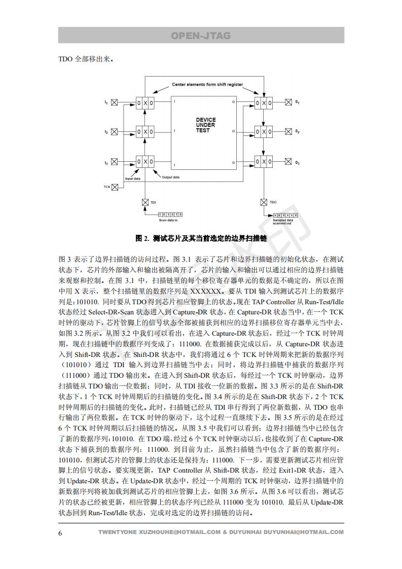
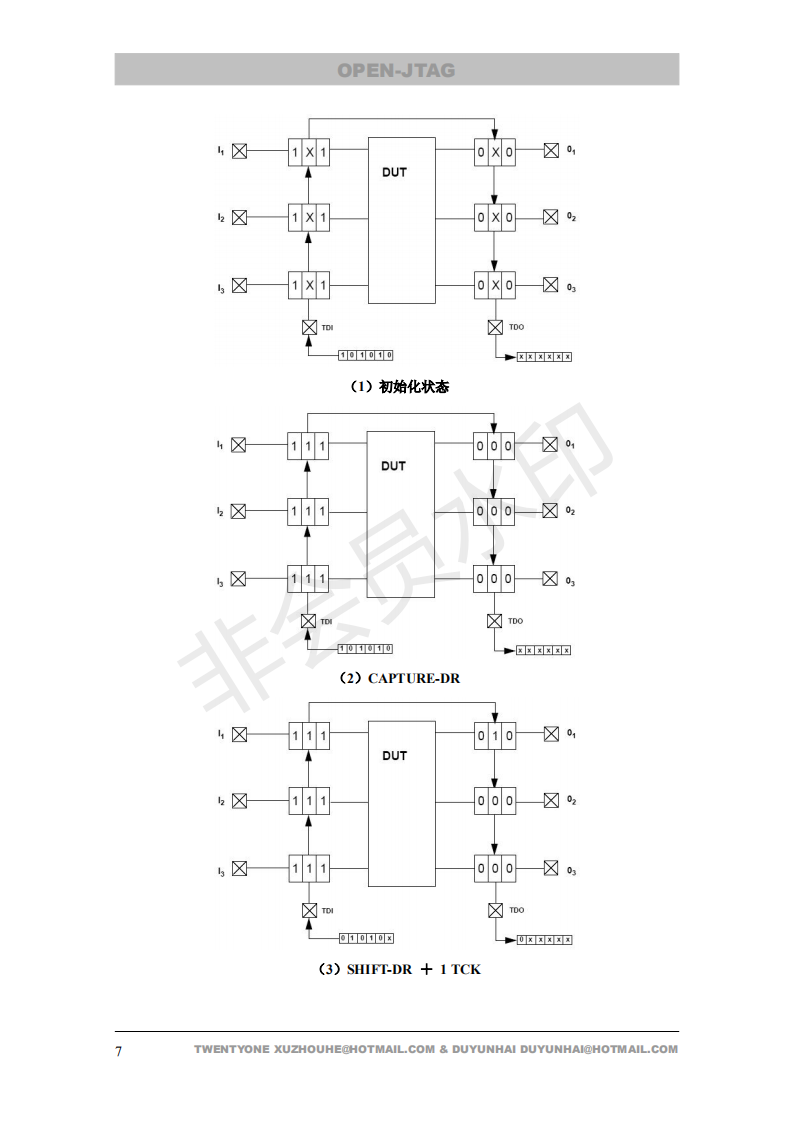
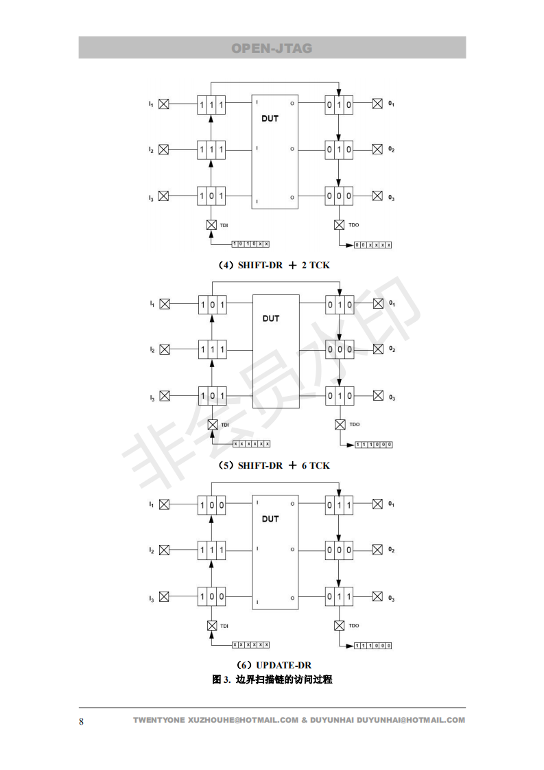
How is JTAG used for chip testing? The main component involved is the boundary scan chain. It is named the boundary scan chain because it is located at the boundary of the processor. We know that the CPU communicates with peripherals through pins, and all data is input or output through these pins, while JTAG achieves chip testing by monitoring the signals on the pins. The boundary scan chain is a component located on the pins. As shown below:

Through the boundary scan chain, when there is a signal input, the boundary scan chain can capture the signal, and when the CPU needs to output a signal, the boundary scan chain can also capture the output signal. Additionally, the boundary scan chain can directly output signals to the outside. Whether capturing or outputting signals, there needs to be an interface to store these signals; TDI and TDO serve this purpose.
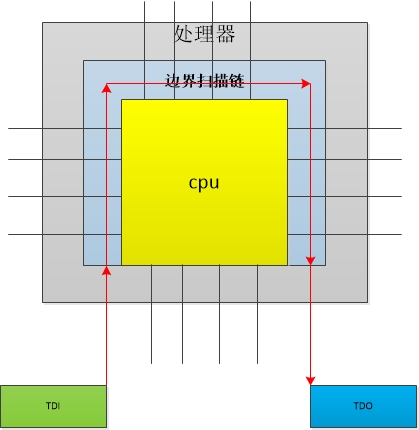
The boundary scan chain stores the signals on the pins. When we input our own signals through the TDI pin, a shifting operation occurs in the direction of the red line above, TDI → boundary scan chain → TDO, allowing us to retrieve the signals from the boundary scan chain via TDO. The signals we input through TDI will also go to the boundary scan chain.
A complete software breakpoint debugging schematic is shown below:
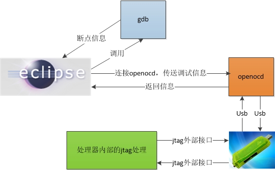
ARM JTAG Debugging Principle
Reference Links
-
Basic Principles and Debugging of JTAG
https://www.cnblogs.com/TaigaCon/archive/2012/12/20/2826941.html-
Definition and Meaning of Various JTAG Interface Pins
https://www.cnblogs.com/jeakon/archive/2012/10/07/2813683.html-
JTAG – Insight into JTAG (the most thorough explanation)
https://www.cnblogs.com/iamlvshijie/archive/2012/04/14/2486189.html
DeeplyRootedInFPGA ExcellentInNeuralNetwork