Follow our public account for timely updates on new articles.
Engineers engaged in hardware, embedded systems, or chip-related fields are likely familiar with JTAG. JTAG primarily has three main uses:
-
Testing and Diagnosis: Initially, the main purpose of JTAG was for testing and diagnosing integrated circuits, used to detect and repair defects in the chip manufacturing process. -
Device Programming: Through JTAG, firmware, configuration files, or programs can be loaded onto chips using a programmer. -
Hardware Debugging: With JTAG, engineers can connect debuggers or emulators to monitor the chip’s status, register values in real-time, and even perform step-by-step execution.
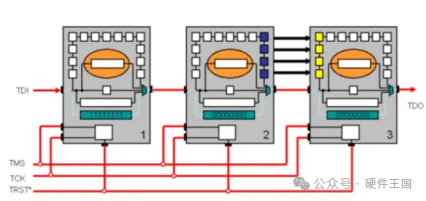
Boundary scan can extend the scanning path to the board level or system level. All information exchanged with the outside (including instructions, test data, and test results) for devices designed based on boundary scan is communicated serially. This allows instructions and related test data to be sent serially to the device, and the execution results of the test instructions to be read out from the device serially. To achieve this functionality, boundary scan technology includes a scan chain composed of boundary scan register units connected to the device pins, allowing control and observation of the device’s boundary signals through scanning test principles, which is the meaning of boundary scan.
Note:
-
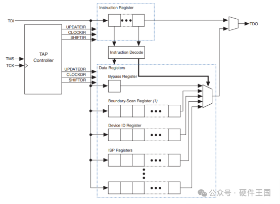
4 dedicated test pins (TCK, TMS, TDI, TDO), collectively referred to as the Test Access Port (TAP). -
1 TAP controller (state machine) with input TCK and TMS, which generates the clock and control signals required for the IR and DR registers (such as shift, capture, and update operations). -
1 n-bit (>=2) instruction register (IR), which stores the current instruction (including Bypass, Identify, Boundary-Scan, and other options). -
The data register includes Bypass, Identify, Boundary-Scan, and other optional registers. -
The boundary scan logic is controlled by the TAP Controller, DR, and IR working together.
Common Instructions
Different instructions constrain the various operations of the boundary scan logic. JTAG instructions appear in binary encoded form. Instruction data is serially shifted into the instruction register from the TDI port on the rising edge of TCK when the TAP controller is in Shift-IR state. Some instructions must be implemented, while others are optional.
|
Instruction Type |
Name |
Selected Register |
Description |
|
Mandatory |
BYPASS |
Bypass |
|
|
EXTEST (External Test) |
Boundary Scan |
External tests, such as interconnect testing between chip pins. |
|
|
SAMPLE (Sampling) |
Boundary Scan |
Sampling, for example, capturing data from the device pins. |
|
|
PRELOAD (Preload) |
Boundary Scan |
Preload, for example, preloading known test data into output pin units. |
|
|
Optional |
INTEST (Internal Test) |
Boundary Scan |
Internal tests, allowing the boundary scan register to serve as the device’s input and output for static testing of the core logic. |
|
IDENTIFY (Device Identification) |
Device Identification |
Places a 32-bit device identification register on the TDI and TDO scan chain to store the manufacturer’s details, version type, and other information. |
|
|
RUNBIST (Built-In Self-Test) |
Designated Test Register |
When the TAP controller is in run-test/idle state, the chip can perform self-tests and place the test results (pass/fail) in designated registers. |
Extest: Primarily used to test connections between ICs or logic circuits outside the boundary scan design. It locks data from the boundary scan register (BSR) into the data register to stimulate the tested connections or external logic circuits, while capturing the responses of the tested connections or external logic circuits under that stimulus. (Before executing the external test instruction, a preload instruction is needed to load the stimulus vector into BSR. After completing the external test instruction, a shift instruction should be used to extract the test results for inspection.)
Boundary Scan Chain
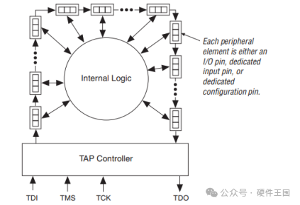
Boundary Scan Register
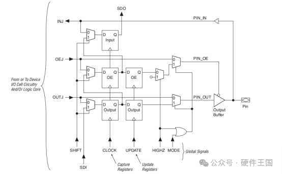
Basic General Boundary Scan Unit
TAP Controller and State Machine:
The next diagram shows the state table of the TAP controller. The values on the state transition arcs represent the TMS values. State transitions occur on the rising edge of TCK, and output values change on the falling edge of TCK.
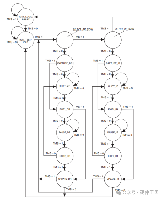
TAP Controller State Machine
Capture-DR:
On the rising edge of TCK, the signal will be “captured” into the corresponding data register unit. If TMS is “0” (triggered by the rising edge of TCK), it enters the Shift-DR state; if TMS is “1”, it enters the Exit1-DR state.
Shift-DR:
Each clock cycle, the previously captured data is sequentially passed through the data register scan chain and finally output serially through TDO. If TMS is “0” (triggered by the rising edge of TCK), it remains in the Shift-DR state; if TMS is “1”, it transitions to Exit1-DR state.
Update-DR:
In the Update-DR state, the data in the data register will be loaded to the corresponding control ports. If TMS is “0”, the TAP Controller returns to the Run-Test/Idle state; if TMS is “1”, the TAP Controller enters the Select-DR-Scan state.
Note:
Where the captured data comes from and where it shifts to can be controlled based on actual applications. For example, if your scan chain logic is mainly used for testing internal logic circuits of the chip, the captured data mainly comes from the internal logic circuit. If used for testing chip pins, signals need to be sent to a specific input pin of the chip through TDI, thus capturing the signal input from TDI. The same applies to updating data.

(If you like this article, scan the code to follow)
Note: Please indicate the source when reprinting
Recommended Classic Articles from This Collection:
01_UART Serial Protocol
02_ Master the I2C Protocol and Applications in One Article