1. Boundary Testing
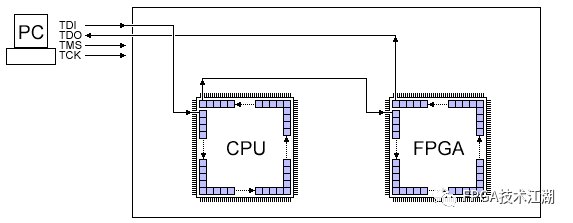
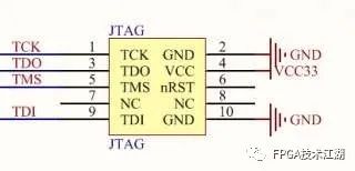
2. JTAG Pins
-
TDI: Test Data Input, data is input to the JTAG port through TDI. -
TDO: Test Data Output, data is output from the JTAG port through TDO. -
TMS: Test Mode Select, used to set the JTAG port to a specific test mode. -
TCK: Test Clock Input. -
TRST: Test Reset.
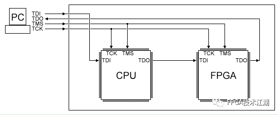
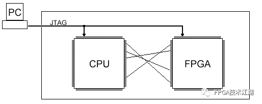
3. How JTAG Works
4. Questions Related to the JTAG Chain
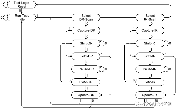
5. Boundary Scan
-
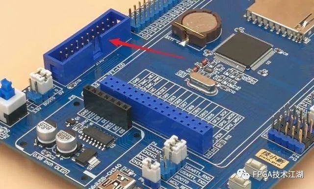
Under the premise that the FPGA development board and related devices are powered off, connect the JTAG download cable; -
Connect the USB Blaster or ByteBlasterII cable; -
Power on the FPGA development board.
-
Turn off the power to the FPGA development board and related devices; -
Disconnect the USB Blaster or ByteBlasterII cable; -
Remove the JTAG download cable and store it in a suitable place.
Due to recent changes in the WeChat public platform push rules, many readers have reported not seeing updated articles in a timely manner. According to the latest rules, it is recommended to frequently click “Recommended Reading, Share, Collect, etc.,” to become a regular reader.
Recommended Reading:
-
iPhone Accused of Falsely Advertising 5G Signal, Experts Provide 4 Reasons!
-
The Popularity of Huawei’s New Phone Stands on the Shoulders of 46 Chinese Suppliers
-
Tested: Huawei Mate X5 Achieves Gigabit Network Speed, Surpassing 5G Levels!
Please click 【See】 to give the editor a thumbs up
