Original: Wolonghui Wolong Village Master
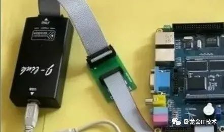
Previously, some netizens asked what the JTAG principle is? Today, I will briefly explain it. JTAG is a debugging, testing, and online programming interface.
JTAG (Joint Test Action Group)
JTAG is an embedded debugging technology used to test chips. Once the circuit board is soldered, how can we ensure that the soldering is correct? Are there any defective chips? These issues are tested through the JTAG testing interface, allowing us to determine the results.
The principle of JTAG is that an interface is encapsulated within the chip, which can be used to test each pin of the chip. It checks whether the functions of each pin are normal. It has a component called a boundary scan chain that can monitor all pins of the chip. Through JTAG testing, we can determine whether the functions of the chip are normal.
The main JTAG test signals include four signals:
TCK: Clock signal
TDI: Input signal
TDO: Output signal
TMS: State select input
TRST: Reset signal
Another function of JTAG is to program chips, such as writing programs directly to FLASH chips soldered on the board through the JTAG interface. However, this is only used temporarily during debugging. In mass production, the program is usually written to FLASH in bulk before PCBA.
Some may argue that this only tests chips and cannot test other circuit components. In fact, the focus is mainly on chips, especially since the defect rate for BGA soldering is typically higher than that of resistors and capacitors. If the chip passes the test, the other components are generally acceptable with modern soldering techniques.
Wolonghui, where masters of the electronics industry gather!