
Instruction Register (IR) 指令寄存器
The purpose of the Instruction Register (IR) is to shift in instructions via the TDI signal. Additionally, the instruction register can hold the current instruction until the new instruction is completely shifted in.
Generally, an IR consists of two registers as shown in Figure 1. The Hold register stores the previous instruction, while the Shift register is used to shift in the next instruction without affecting the previous instruction.
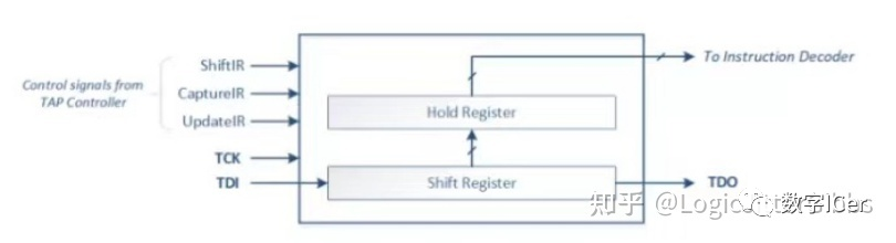
The control signals for the instruction register come from the TAP controller, and the specific control signal values depend on the current state of the FSM state machine, enabling the instruction register to shift in/out instructions (i.e., the serial update process in Shift-IR state) or to transfer the contents of the Shift register to the Hold register (i.e., the parallel update process in Update-IR state).
Assuming a 4-bit length instruction register, if we want to load a value, for example, 4’b1100, the following steps are required:
-
Control the TMS signal to input the following sequence, transitioning the state machine from the “Test Logic Reset” state to the “Shift-IR” state:
-
TMS = 0 (1st clock) -
TMS = 1 (2nd clock) -
TMS = 1 (3rd clock) -
TMS = 0 (4th clock) -
TMS = 0 (5th clock)
-
During the “Shift-IR” state, keep TMS = 0 for the next 3 clock cycles and serially shift in the instruction value (4’b1100) via TDI. NOTE: Using 3 clock cycles to shift in 4 bits of data is because the LSB (bit 0) of the data 4’b1100 appears on the TDI port after the fourth clock cycle, allowing the FSM to shift in the LSB when it enters the “Shift-IR” state in the fifth clock cycle. Ultimately, the last bit MSB of the data will be shifted in during the eighth clock cycle.
-
Control the TMS signal to input the following sequence, transitioning the state machine from the “Shift-IR” state to the “Update-IR” state:
-
When the FSM enters the “Update-IR” state, the value in the Shift register (4’1100) will be loaded in parallel to the Hold register. At this point, the instruction can be read by the instruction decoder.
-
TMS = 1 (9th clock) -
TMS = 1 (10th clock)
Instruction Decoder 指令译码器
The instruction in the Instruction Register (IR) is transmitted to the instruction decoding logic, which selects the target data register for the next JTAG operation based on the instruction.
We assign a different opcode value to each data register. When a specific data register is selected, its corresponding instruction is loaded into the instruction register, and then the instruction decoder decodes the opcode and establishes a path between TDI/TDO and the corresponding data register.
Assuming our JTAG module has two data registers DR-1 and DR-2, along with a 4-bit wide instruction register. We will assign an opcode and corresponding instruction to each data register, for example:
-
DR-1 ( opcode = 4’b0010) -
DR-2 ( opcode = 4’b0011)
NOTE: A 4-bit opcode is used because this JTAG instruction decoder has a width of 4 bits.
If we want to access DR-2 via JTAG, we need to load the value 4’b0011 into the instruction decoder, which will decode this value and select DR-2.
Translation Author: Zhihu LogicJitterGibbs Original link: https://vlsitutorials.com/jtag-architecture-overview/

Previous Recommendations
SoC Design: Bus Interface
SoC Design: Low Power
Application of Perl in IC
EDA Tutorials
Chip Design
UVM Chip Verification
FPGA Series
Vivado Advanced
Formal Verification
Digital C Written Exam
Digital IC Interview Experience
Excellent IC/FPGA Open Source Projects
Synthesis and Timing Analysis
Statement: Reproduction without authorization is prohibited