JTAG (Joint Test Action Group) is an interface established by a group called the JTAG group, founded in 1985. In 1990, IEEE deemed everything appropriate and released IEEE Standard 1149.1-1990, named the Standard Test Access Port and Boundary-Scan Architecture, which is the renowned JTAG.
Do you know the three main functions of JTAG? They are:
1. A downloader, which downloads software into FLASH.
2. DEBUG, similar to a doctor’s stethoscope, it can probe the internal thoughts of the chip.
3. Boundary scan, which can access the logical states of signals inside the chip, as well as the states of the chip pins, etc.
There is no standard interface definition for JTAG; even each company has different definitions. In ARM’s System and Interface Design Reference documentation,
Document download link:
Link: https://pan.baidu.com/s/13aQXOXR73_wiERz2kwN15w
Extraction code: xaaf
(Tip: The public account does not support external links, please copy the link to the browser to download)
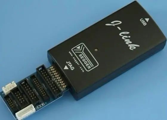
The image we often see on the internet is the JTAG interface of SEGGER company’s Jlink.
J-Link is a debugger based on JTAG launched by the German SEGGER company. In simple terms, it is a JTAG protocol converter box, which is a small USB to JTAG conversion box that connects to the computer via the USB interface, while connecting to the target board internally using the JTAG protocol. It completes the work of converting from software to hardware.
At the same time, Jlink is also considered the most popular debugger. According to the System and Interface Design Reference, this ARM official JTAG 20pin is not the same.
Here, I hope everyone understands the relationship between ARM, Jlink, and JTAG.
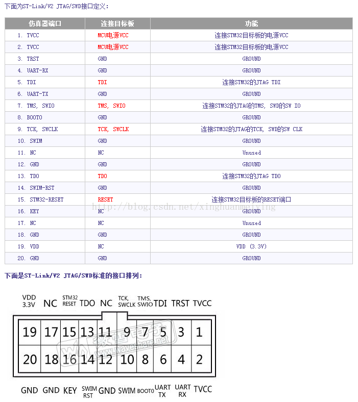
The interface of ST-link V2 is also used frequently. As mentioned above, this is also an interface defined by ST company, as shown below:
Ulink, CMSIS_DAP, and other STM32 debuggers follow the same principle.
Boundary Testing:
For example, if you have two chips connected by many wires, how can you ensure the connections between these wires are OK? You can use JTAG, which can control all the IC pins. This is called chip boundary testing.
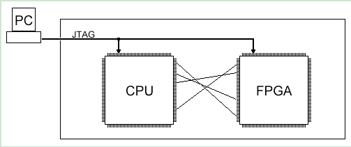
In the JTAG interface, the most commonly used signals are four: TCK/TMS/TDO/TDI. The JTAG interface can be used one-to-one or can form a daisy chain in a one-to-many topology structure, as shown in the two diagrams below. In multi-core chips, the chip’s internal connections are already in a daisy chain format.
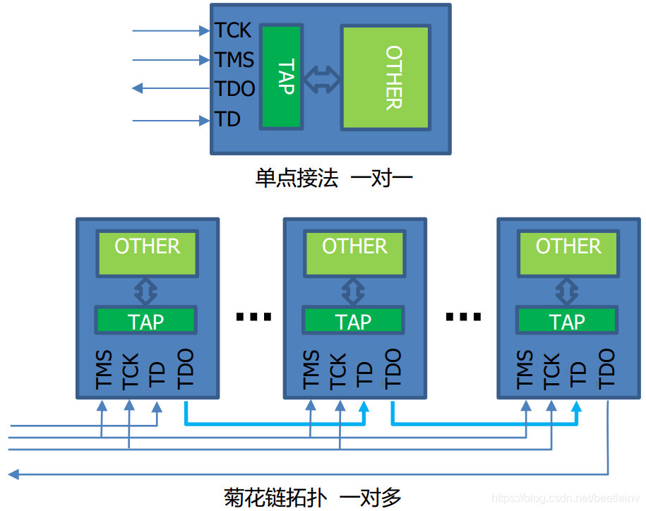
JTAG daisy chains have many applications.
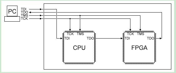
CPU and FPGA manufacturers allow JTAG to be used for port debug; FPGA manufacturers allow configuration of FPGA through JTAG, using JTAG signals to enter the FPGA core.
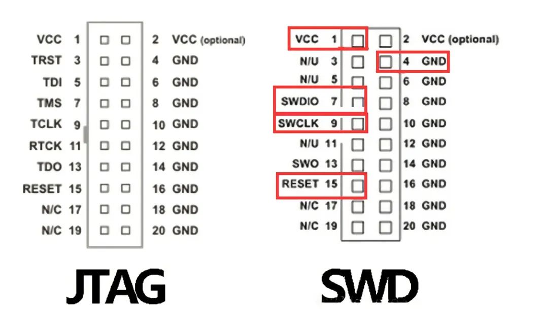
SWD interface: Serial Wire Debug (SWD) can be considered a different debugging mode from JTAG, which is directly reflected in the debugging interface. Compared to JTAG‘s 20 pins, SWD only requires 4 (or 5) pins.
VCC, SWDIO, SWCLK, GND (in some cases, the RESET pin is also added).
The differences between SWD and traditional debugging methods:
-
SWD mode is more reliable than JTAG in high-speed modes. In cases of large data volumes, JTAG program downloads may fail, while this occurrence is much less likely with SWD. Generally, if you are using JTAG emulation mode, you can directly use SWD mode as long as your emulator supports it, so it is recommended to use this mode.
-
When the CPU‘s GPIO pins are insufficient, you can use SWD emulation, which supports fewer pins.
-
In cases where the hardware PCB size is limited, it is recommended to use SWD mode, which requires fewer pins, thus requiring less PCB space. You can choose a very small 2.54 pitch 5 pin terminal for the emulation interface.
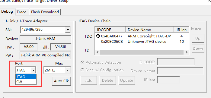
In the Keil environment, the Jlink debugger’s JTAG mode and SWD mode
In the IAR environment, the Jlink debugger’s JTAG mode and SWD mode
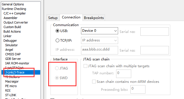
Comparison of Jlink’s JTAG mode and SWD mode
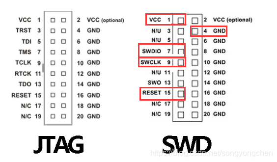
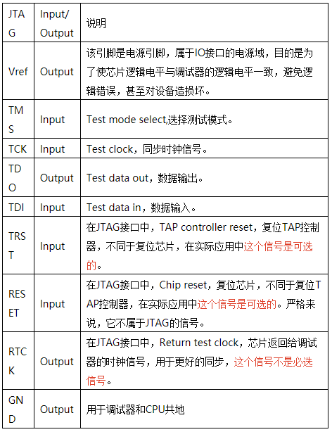
JTAG pin description
SWD pin description
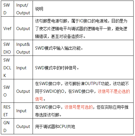
We mentioned the Vref pin, which belongs to the power domain of the IO interface, aimed at ensuring that the chip logic level is consistent with the debugger’s logic level to avoid logical errors and even damage to the device.
On the Jlink, there is a Vref jumper cap.
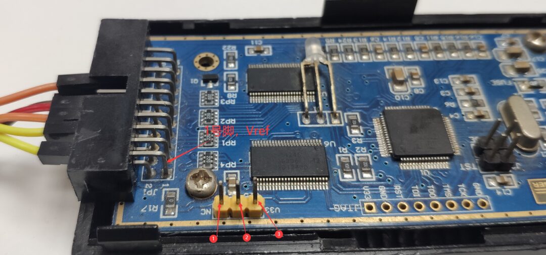
Three pins: ① is NC, ② is Vref, which is connected to the output’s 1 pin, and ③ is 3.3V
If you want the Jlink to output 3.3V on pin 1, simply short connect ② and ③.
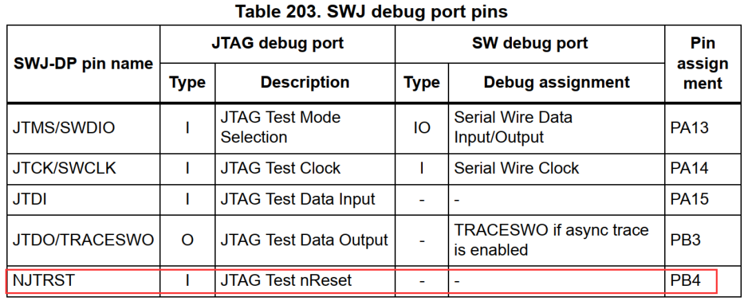
The TRST pin defined in JTAG is used to reset the TAP controller. In the STM32 series microcontroller, there is no TRST pin, it is named NJTRST.
For example, in the STM32F207, the NJTRST pin is described in both JTAG and SWD modes.
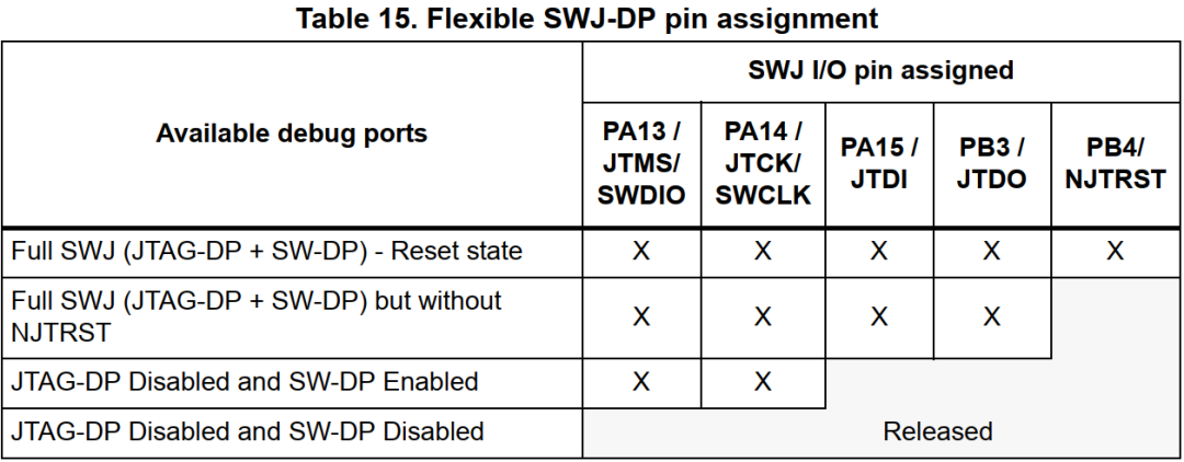
Availability of the SWJ I/O pin in STM32F207
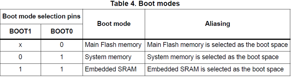
In some STM32 product emulations, using 4 line SWD mode, the release version usually sets the JTAG port as a normal IO, or due to insufficient pins, it is used for other purposes in the release version. When debugging the release version, since the JTAG mode is disabled, there is no way to emulate.
This is when the most common practice is to pull up the BOOT0 pin to enter the Main Flash memory mode for debugging emulation.
Compared to the official development board of STM32, when using SWD mode without exposing the RST pin, of course, the SWD also includes the SWO signal, which is for monitoring and is also very useful. Both signals can be connected to the emulator.
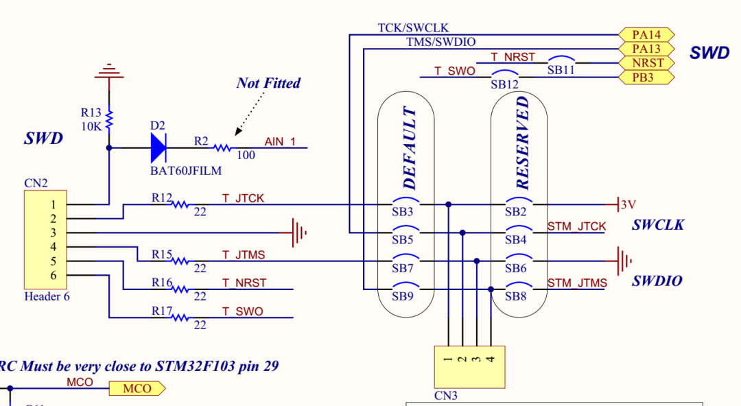
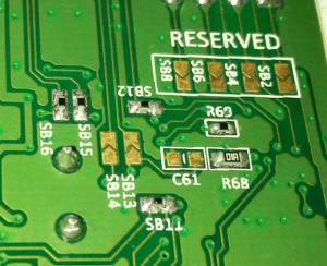
On the board:
The emulator has an Under Reset mode, so the emulator will send the RST signal to the MCU when emulation is needed, putting the MCU in the RST state, or using reset after emulation, where the code has not yet reached the disabled JTAG state, allowing for direct emulation. Of course, you can also actively reset the power supply to detach from the original JTAG disabled state. You can also pull up the BOOT0 pin.