
Welcome to the new column “Today’s Law” in the FPGA technology world. Of course, we are not here to study laws and regulations. So what are we discussing? We are discussing some small details and methods in product development and technical learning. Everyone is welcome to learn and communicate together. If you have good ideas or articles, please submit them, indicating your pen name and related articles. Submission email: [email protected]. Today we bring you “Who Touched My JTAG Port?” Without further ado, let’s get started.
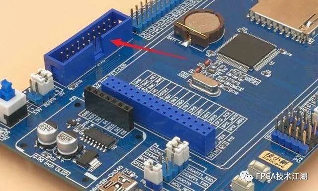
In the process of FPGA development and learning, a key step is the board programming, and achieving hardware “hard presence” is crucial. Generally speaking, the JTAG port is more commonly used, so I believe some of you have encountered issues with the JTAG port malfunctioning or being damaged and unable to be used. Recently, I encountered such a situation where the JTAG port of the FPGA suddenly could not download programs, and this was not the first time. It happened similarly during a previous project; it was working well one day and then stopped the next day, which was quite frustrating. Therefore, I tried many solutions, and initially did not consider that the JTAG port was broken. Consequently, I replaced the USB blaster, but there was no response at all. Could it really be that the JTAG port was broken? I then researched related materials to clarify the essence of the problem. Below are some of my findings, shared for your reference and discussion.
Based on the materials I researched and my practical experience, during the use of the JTAG download interface, please do not plug and unplug with power on, as it may damage the JTAG signal pins of the FPGA chip. So how do you confirm if the JTAG port is damaged? First, you need to eliminate a few basic factors: First, check if the connections are matching. Many devices correspond to many interfaces, and under actual conditions, they must be matched correctly, otherwise, the above situation may occur; Second, rule out problems with the download cable. If the download cable is faulty, you can try multiple download cables to eliminate this type of issue. If you still cannot access the FPGA’s JTAG port, it is very likely that the JTAG port of your FPGA chip is damaged. At this point, please use a multimeter to check if TCK, TMS, TDO, and TDI are shorted to GND. If any signal is shorted to ground, it indicates that the JTAG signal pins are damaged.
As for what the JTAG port is, let’s discuss it here. JTAG stands for Joint Test Action Group.
JTAG is an IEEE standard used to solve board-level issues, originating in the 1980s. Today, JTAG is used for programming, debugging, and probing ports. Of course, its original use was boundary testing.
1. Boundary Testing
For example, if you have two chips connected by many wires, how do you ensure that these wires are connected correctly? Using JTAG, it can control all IC pins. This is called chip boundary testing.
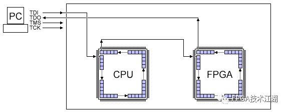
2. JTAG Pins
JTAG has evolved to have pins, typically four pins: TDI, TDO, TMS, TCK, and there is also a reset pin TRST. The JTAG pins on the chip are actually dedicated.
-
TDI: Test Data Input, data is input to the JTAG port through TDI; -
TDO: Test Data Output, data is output from the JTAG port through TDO; -
TMS: Test Mode Select, used to set the JTAG port to a specific test mode; -
TCK: Test Clock Input; -
TRST: Test Reset.
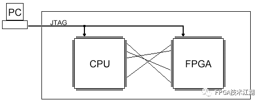
CPU and FPGA manufacturers allow JTAG for port debugging; FPGA vendors allow configuration of FPGAs through JTAG, using JTAG signals to enter the FPGA core.
3. How JTAG Works
The PC controls JTAG: connect the JTAG cable to the PC’s parallel port, USB, or network port. The simplest is to connect to the parallel port.
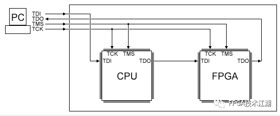
TMS: Inside each chip with JTAG, there is a JTAG TAP controller. The TAP controller is a state machine with 16 states, and TMS is the control signal for this. When TMS connects all chips together, the TAP state transitions of all chips are synchronized. Below is a diagram of the TAP controller:
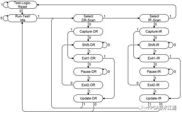
Changing the value of TMS will cause state transitions. If a high level is maintained for 5 cycles, it will jump back to test-logic-reset, usually used to synchronize the TAP controller; the two most important states are Shift-DR and Shift-IR, which connect TDI and TDO.
IR: Instruction Register, you can write values to this register to notify JTAG to do something. Each TAP has only one IR register and its length is fixed.
DR: TAP can have multiple DR registers, similar to IR registers, each IR value selects a different DR register. (Very confusing)
4. Questions Related to JTAG Chain
Calculating the number of ICs in the JTAG chain:
An important application is when the IR value is all ones, indicating the BYPASS command. In BYPASS mode, the DR register in the TAP controller is always a single bit, from input TDI to output TDO, usually one cycle, doing nothing.
The number of ICs can be calculated using BYPASS mode. If the TDI-TDO chain delay of each IC is one clock, we can send some data and detect how long it takes to delay, then we can estimate the number of ICs in the JTAG chain.
Getting the device ID in the JTAG chain:
Most JTAG ICs support the IDCODE command. In the IDCODE command, the DR register will load a 32-bit value representing the device ID. Unlike the BYPASS instruction, there is no standard IR value in the IDCODE mode. However, each time the TAP controller jumps to the Test-Logic-Reset state, it will enter IDCODE mode and load IDCODE into DR.
5. Boundary Scan:
When the TAP controller enters boundary scan mode, the DR chain can traverse each IO block or read or intercept each pin. When using JTAG on FPGA, you can know the status of each pin when the FPGA is running. You can use the JTAG command SAMPLE, although different ICs may vary.

This article does not delve deeply into the principles of JTAG debugging, but for those interested, you can obtain detailed documents to review the principles of JTAG debugging.
Link: https://pan.baidu.com/s/1PbBFgWnZgROeIiYhscBuZw
Extraction code: 0u5a
If the JTAG port is damaged, then one can only “mourn the loss”. However, do not only focus on sadness; the most important thing is to analyze the reasons behind it. The same principle applies to other tasks. Let’s analyze: during our use, we often plug and unplug the JTAG download port casually for convenience. In most cases, no problems occur. However, there remains a small chance of the following issues: static electricity and surges caused by hot plugging the JTAG port can eventually lead to breakdown of the FPGA pins. Additionally, some suspect that counterfeit USB Blasters or ByteBlasterII designs simplify by removing protective circuits. However, feedback from many practical situations proves that original USB Blasters can also have the same issue. Some have questioned whether ALTERA’s low-end chips lack diode clamping protection circuits to reduce costs in FPGA’s IO units. Such doubts do not address the essence of the problem. The most important thing is to standardize operations and minimize the premature end of hardware devices or interfaces due to improper operation. Now, how should we standardize the operation of the JTAG download port?
Power-on operation process:
-
1. With the FPGA development board and related devices powered off, plug in the JTAG download cable; -
2. Plug in the USB Blaster or ByteBlasterII cable; -
3. Turn on the power of the FPGA development board.
Power-off operation process:
-
1. Disconnect the power of the FPGA development board and related devices; -
2. Disconnect the USB Blaster or ByteBlasterII cable; -
3. Unplug the JTAG download cable and store it in a suitable place.
Although the above operational steps may seem cumbersome, and sometimes we may take them lightly, to ensure that the chip is not damaged, it is recommended to follow the steps as outlined. The issue I encountered above was due to TCK being shorted to GND. Although the occurrence probability is not high, to reasonably and sustainably use hardware-related devices, it is still advisable to operate systematically. Changing perspectives, “more practice” is also beneficial. Finally, I would like to remind you that it is best not to hot plug the JTAG download port with power on, as it can help prolong the life of the JTAG port. After all, long-term companionship is quite nice, and we should not wait until we lose it to feel regret.
Selected Articles from Previous Issues


Summary | FPGA Zero-Basis Learning Series
FPGA Chip Industry Popular Science
Master FPGA VHDL in One Week Day 7 and Summary
Master FPGA Verilog HDL Syntax in One Week Summary
Timing Analysis Theory and Timequest Usage_Chinese Electronic Version
Resource Summary Update | FPGA Software Installation Packages, Books, Source Code, Technical Documents… (Updated on 2021.01.04)


FPGA Technology Community Broadly Issues Community Posts
Ad-free pure mode, providing a clean space for technical exchanges, from beginner to industry elite, from military industry to civilian enterprises, covering various fields such as communication, image processing, and artificial intelligence, providing a pure and professional technical exchange learning platform.
FPGA Technology Community WeChat Group

Add the group owner’s WeChat, note your profession + direction + name to join the group
FPGA Technology Community QQ Group

Note your area + profession + direction + name to join the group