
Interface Name: JTAG
Full English Name: Joint Test Action Group
Chinese: 联合测试工作组
Standard Number: IEEE1149.1-1990/IEEE1149.1a-1993
Standard Maintenance: IEEE
Current Specification: www.IEEE.org
Latest Version: IEEE1149.1-2013 Standard Test Access Port and Boundary-Scan Architecture
Effective Date: 2013
Next Version: TBD
Description: JTAG is an international standard testing protocol (IEEE 1149.1 compatible), primarily used for internal testing of chips. The standard JTAG interface consists of 4 lines: TMS, TCK, TDI, and TDO, which are mode select, clock, data input, and data output lines, respectively. It is a chip testing technology interface.
JTAG is a working group under IEEE that studies the standard test access interface and boundary-scan architecture. The predecessor of JTAG was JETAG (Joint European Test Action Group).
1. Interface Structure
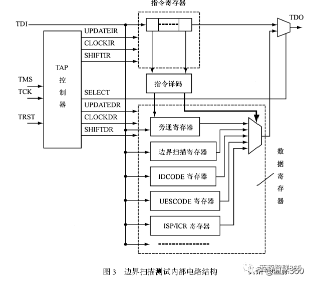
For chips that support JTAG interfaces, their internal structure is shown in the figure below. TAP (Test Access Port) is a universal port that allows access to all data registers (DR) and instruction registers (IR) provided by the chip. When there are multiple BSCs inside the chip, there needs to be a corresponding mechanism to control access. Control of the entire TAP is accomplished through the TAP Controller.
TMS is the Test Mode Select, which controls the state of the JTAG state machine through the TMS signal;
TCK is the clock signal for JTAG, TDI is the data input signal, TDO is the data output signal, and nTRST is the JTAG reset signal, which resets the JTAG state machine and the internal macro cell.
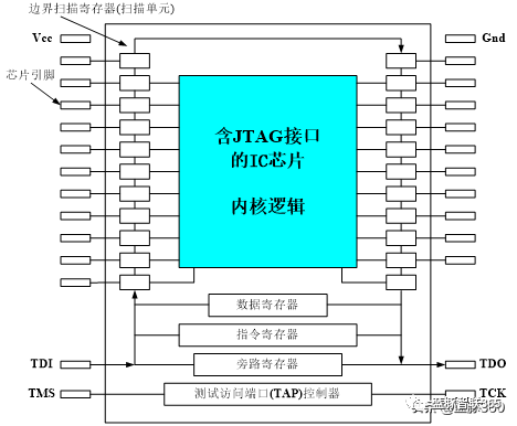

JTAG Pin Definitions
TCK – Test Clock Input;
TDI – Test Data Input, data is input to the JTAG port via TDI;
TDO – Test Data Output, data is output from the JTAG port via TDO;
TMS – Test Mode Select, TMS is used to set the JTAG port to a specific test mode.
Optional Pin TRST – Test Reset, input pin, active low.
2. Working Principle
The basic principle of JTAG is to define a TAP (Test Access Port) inside the device, allowing testing of internal nodes through dedicated JTAG testing tools.
² Facilitates fault location in chips, quickly and accurately tests whether the connection between two chip pins is reliable, improving testing efficiency.
² Chips with JTAG interfaces have built-in predefined functional modes, allowing the chip to be placed in a specific functional mode through boundary scan channels, thereby enhancing system control flexibility and facilitating system design.
JTAG testing allows multiple devices to be connected in series through the JTAG interface, forming a JTAG chain, enabling individual testing of each device. Nowadays, JTAG interfaces are also commonly used for implementing ISP (In-System Programmer) to program devices like FLASH.
JTAG programming is online programming; in traditional production processes, chips are pre-programmed before being mounted on the board. The simplified process is to fix the device to the circuit board first and then program it using JTAG, greatly accelerating project progress. The JTAG interface can program all components inside DSP chips.
JTAG has an internal state machine known as the TAP controller. The TAP controller’s state machine changes states via TCK and TMS, enabling data and instruction input.
Boundary Scan
The basic idea of boundary scan technology is to add a shift register unit near the chip’s input/output pins. Since these shift register units are distributed along the edges of the chip, they are called Boundary-Scan Register Cells. Boundary scan testing is implemented through boundary scan units and some additional testing control logic. When the chip is in debug mode, these boundary scan registers can isolate the chip from the surrounding input/output. Through these boundary scan register units, observation and control of the chip’s input/output signals can be achieved.
In normal operating conditions, these boundary scan registers are transparent to the chip, so normal operation is not affected.
The JTAG standard defines a serial shift register. Each unit of the register is assigned to the corresponding pin of the IC chip. Each independent unit is called a BSC (Boundary-Scan Cell). This series of BSCs forms a JTAG loop inside the IC, and all BSRs (Boundary-Scan Registers) are activated through JTAG testing, while these pins maintain normal IC functionality.
Each I/O pin has a BSC, and each BSC has two data channels: one is the test data channel, which includes test data input (TDI) and test data output (TDO); the other is the normal data channel, which includes normal data input (NDI) and normal data output (NDO). As shown in Figure 1.
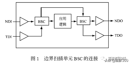
In normal operating conditions, input and output data can freely pass through each BSC, with normal operational data entering from NDI and exiting from NDO. In test mode, the data flow channel can be selected: for input IC pins, data can be input from either NDI or TDI; for output IC pins, data can be output from BSC to NDO or from BSC to TDO.
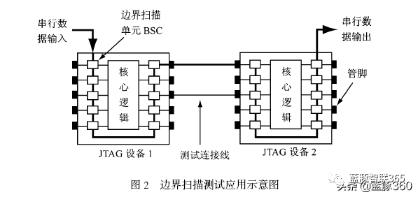
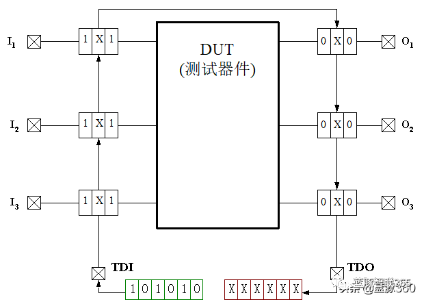
Additionally, the boundary scan register units on the chip’s input/output pins can be interconnected, forming a boundary scan chain around the chip. Generally, chips will provide several independent boundary scan chains to achieve complete testing functionality. The boundary scan chain can serially input and output data, and with the corresponding clock and control signals, the chip in debug mode can be easily observed and controlled.
Figure 2 shows a schematic of boundary scan testing applications. To test the connection between two JTAG devices, first set the BSC of a specific output test pin of JTAG device 1 to high or low, output to NDO, and then let the input test pin of JTAG device 2 capture the NDI value from the pin. The captured data is then output to TDO through the test data channel, and by comparing the test results, a quick and accurate judgment of the reliability of the connection between these two pins can be made.
JTAG Controller
The JTAG controller mainly consists of three parts:
l Test Access Port (TAP) controller
l Instruction register (including instruction decoder)
l Data register
The TAP controller is the core controller for boundary scan testing. TAP has the following 5 control signals:
n TCK: TCK provides an independent, basic clock signal for TAP operations; all operations of TAP are driven by this clock signal. TCK is mandatory in the IEEE 1149.1 standard.
n TMS: The TMS signal is used to control the state transitions of the TAP state machine. The TMS signal can control the TAP to transition between different states. The TMS signal is valid on the rising edge of TCK. TMS is mandatory in the IEEE 1149.1 standard.
n TDI: TDI is the data input interface. All data to be input into a specific register is serially input one bit at a time through the TDI interface (driven by TCK). TDI is mandatory in the IEEE 1149.1 standard.
n TDO is the data output interface. All data to be output from a specific register is serially output one bit at a time through the TDO interface (driven by TCK). TDO is mandatory in the IEEE 1149.1 standard.
n TRST: TRST can be used to reset (initialize) the TAP Controller. However, this signal interface is optional in the IEEE 1149.1 standard and is not mandatory. TAP can also be reset (initialized) through TMS.
Internally, the TAP controller has multiple registers: JTAG control instruction register, test data register, bypass register (BYPASS), device identification code (IDCODE) register, and scan path selection register, among others.
Instruction Register: If executing boundary scan testing for the data register, the instruction register is responsible for providing addresses and control signals to select a specific data register; it can also execute boundary scan testing through the instruction register, where the SELECT signal output from TAP drives TDO.
Data Register: The boundary scan chain is a very important type of data register. IEEE 1149.1 mandates two data registers: Boundary Scan Register and BYPASS Register. Other registers are optional. The instruction register selects a specific data register as the boundary scan test register, and when a scan path is selected, other paths are in a high impedance state. The Boundary Scan Register consists of a series of BSCs surrounding the IC pins, which is used to implement the input and output of test pin signals; the BYPASS Register consists of just one scan register bit, and when the bypass register is selected, there is only one register between TDI and TDO, effectively not executing boundary scan testing. The purpose of the bypass register is to shorten the scan path for ICs that do not need to be tested.
As mentioned above, the TAP controller can choose to use the instruction register scan or data register scan under the control of TCK and TMS, as well as control the various states of boundary scan testing. TMS and TDI are sampled on the rising edge of TCK, while TDO changes on the falling edge of TCK.
TAP Control State Machine
The TAP controller’s state machine has a total of 16 states, but only 6 stable states: Test Logic Reset, Run-Test/Idle, Shift-DR, Pause-DR, Shift-IR, Pause-IR. The other states are not stable states but are only transient.
At power-up or during normal operation of the IC, TMS must be held high for at least 5 TCK cycles for TAP to enter the Test Logic Reset state. At this time, TAP sends a reset signal so that all testing logic does not affect the normal operation of the component. If boundary scan testing is required, it can exit the reset state under the control of TMS and TCK to enter the various states needed for boundary scan testing.

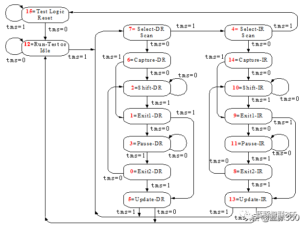
Instruction Register Access Process:
u Power on the system, the TAP Controller enters the Test-Logic Reset state.
u Run-Test/Idle -> Select-DR-Scan -> Select-IR-Scan -> Capture-IR -> Shift-IR -> Exit1-IR -> Update-IR, finally returning to the Run-Test/Idle state.
u In the Capture-IR state, a specific logic sequence is loaded into the instruction register; then it enters the Shift-IR state.
Data Register Access Process:
u The currently accessible data register is determined by the current instruction in the instruction register.
u Starting from Run-Test/Idle, sequentially enter Select-DR-Scan -> Capture-DR -> Shift-DR -> Exit1-DR -> Update-DR, finally returning to the Run-Test/Idle state.
n JTAG Scan Chain Working Principle:
Each scan unit internally consists of two D flip-flops and two multiplexers.
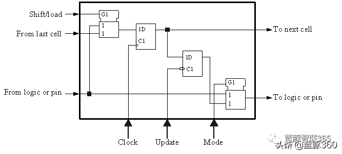
In the normal state, i.e., suspended, BSR is transparent to the chip and does not affect the chip’s normal operation.
When the chip is in debug mode, BSR isolates the chip from the surroundings. Through BSR, observation and control of the chip’s pins can be achieved.
For input pins, signals (data) can be loaded to the pins through BSR operations.
For output pins, the output signals on the pins can be