“SPI is a synchronous serial communication interface that achieves full-duplex transmission with 4 lines. FPGA can flexibly adapt to different rates and communication modes. This article first explains its core principles and four protocol modes, then provides a loopback test scheme for Mode 0, including sending, receiving, and top-level module design and constraints, simulating to verify timing compliance and data consistency, providing a reliable reference for SPI applications.”
01
—
SPI Communication Principles
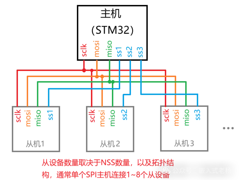
SPI (Serial Peripheral Interface) is a synchronous serial communication interface that relies on the master device (such as FPGA) to generate a synchronous clock SCLK, controlling full-duplex transmission of data between the master output (MOSI, Master Out Slave In) and the slave output (MISO, Master In Slave Out). The chip select signal SS (active low) selects the target slave device, avoiding data interference among multiple slave devices. The SPI controller implemented in FPGA consists of a clock divider unit, a serial-to-parallel shift module for sending, and a parallel-to-serial shift module for receiving. It requires only 4 signal lines (SCLK, MOSI, MISO, SS) to complete data interaction, supporting low-speed peripheral control (such as driving a digital tube) and high-speed data acquisition (such as ADC sampling), and can flexibly adapt to different transmission rates and communication modes through logic code.
02
—
SPI Communication Protocol
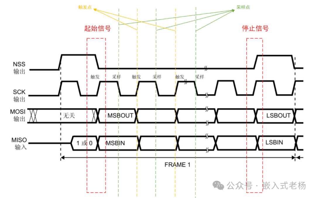
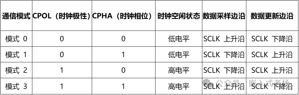
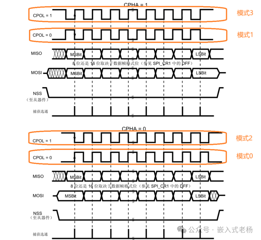
The SPI protocol defines four communication modes through the combination of clock polarity (CPOL) and clock phase (CPHA), ensuring timing synchronization between the master and slave devices. CPOL determines the idle state level of SCLK (0 for low, 1 for high), while CPHA determines the data sampling edge (0 for the first clock edge, 1 for the second clock edge); the communication process is initiated by pulling SS low, sampling/updating data on the specified edge of SCLK, and ends when SS is pulled high. A single byte transmission includes 1 start bit (SS low), 8 data bits, and 1 stop bit (SS high), supporting continuous multi-byte transmission.
03
—
SPI Loopback Test Case
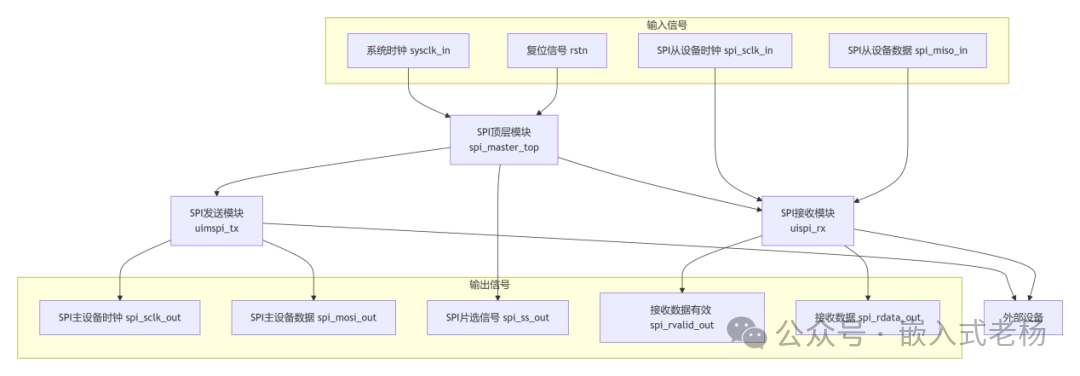
This case implements reliable communication verification conforming to SPI Mode 0 (CPOL=0, CPHA=0): the top-level module precisely controls the chip select timing through a state machine (pulling spi_ss_out low to select the slave device before sending, and pulling it high to deselect after sending), avoiding interference from unrelated data; the sending module converts incrementing data (0→1→2…) into serial signals output from spi_mosi_out, while the receiving module receives data through spi_miso_in in a loopback manner, activating the receiving logic only when the chip select is low, and finally indicating valid data reception through the spi_rx_valid_out signal.
1. SPI Sending Module (ui_mspi_tx.v)
module uimspi_tx#( parameter CLK_DIV = 100, // System clock division factor: CLK_DIV = System clock/SPI clock - 1 parameter CPOL = 1'b0, // SPI clock polarity: 0=idle low, 1=idle high parameter CPHA = 1'b0 // SPI clock phase: 0=sample on first edge, 1=sample on second edge)( input wire clk_in, // System clock input input wire rstn, // Reset signal, active low output reg spi_mosi_out, // SPI data output (MOSI) output reg spi_sclk_out, // SPI clock output input wire spi_tx_req_in, // SPI send request input input wire [7:0] spi_tx_data_in,// SPI parallel send data input output reg spi_busy_out // SPI send busy signal output);localparam LP_SPI_DIV = CLK_DIV; // Total SPI clock division factorlocalparam LP_SPI_DIV_HALF = LP_SPI_DIV / 2; // SPI clock half-cycle division factorlocalparam LP_TX_BIT_CNT_MAX = 4'd8; // Maximum number of bits to send (8 bits data)reg [9:0] clk_div_r; // Clock division registerreg spi_en_r; // SPI send enable registerreg [3:0] tx_bit_cnt_r; // Bit count register for sending (0~8)reg [7:0] spi_tx_data_r; // SPI send data buffer registerwire clk_en_half; // Half-cycle clock enable (rising edge)wire clk_en_full; // Full-cycle clock enable (falling edge)wire clk_end; // Send end flagreg spi_strobe_en_r; // SPI data shift enable registerwire spi_strobe; // SPI data shift trigger signalassign clk_en_half = (clk_div_r == LP_SPI_DIV_HALF);assign clk_en_full = (clk_div_r == LP_SPI_DIV);assign clk_end = clk_en_half && (tx_bit_cnt_r == LP_TX_BIT_CNT_MAX);// Clock division logicalways @(posedge clk_in or negedge rstn) begin if (!rstn) begin clk_div_r <= 10'd0; end else if (spi_en_r) begin clk_div_r <= (clk_div_r < LP_SPI_DIV) ? (clk_div_r + 1'b1) : 10'd0; end else begin clk_div_r <= 10'd0; endend// SPI clock generation logicalways @(posedge clk_in or negedge rstn) begin if (!rstn) begin spi_sclk_out <= CPOL; end else if (spi_en_r) begin spi_sclk_out <= clk_en_full ? 1'b0 : (clk_en_half && (tx_bit_cnt_r < LP_TX_BIT_CNT_MAX)) ? 1'b1 : spi_sclk_out; end else begin spi_sclk_out <= CPOL; endend// Bit count logicalways @(posedge clk_in or negedge rstn) begin if (!rstn || !spi_en_r) begin tx_bit_cnt_r <= 4'd0; end else if (clk_en_half) begin tx_bit_cnt_r <= tx_bit_cnt_r + 1'b1; endend// Data shift enable logicalways @(posedge clk_in or negedge rstn) begin if (!rstn) begin spi_strobe_en_r <= 1'b0; end else if (tx_bit_cnt_r < LP_TX_BIT_CNT_MAX) begin spi_strobe_en_r <= (clk_en_half) ? 1'b1 : spi_strobe_en_r; end else begin spi_strobe_en_r <= 1'b0; endend// SPI data shift logicassign spi_strobe = CPHA ? (clk_en_half && spi_strobe_en_r) : (clk_en_full && spi_strobe_en_r);always @(posedge clk_in or negedge rstn) begin if (!rstn || clk_end) begin spi_en_r <= 1'b0; spi_tx_data_r <= 8'h00; end else if (spi_tx_req_in && !spi_en_r) begin spi_en_r <= 1'b1; spi_tx_data_r <= spi_tx_data_in; end else if (spi_en_r && spi_strobe) begin spi_tx_data_r <= {spi_tx_data_r[6:0], 1'b1}; endend// Busy signal output logicalways @(posedge clk_in or negedge rstn) begin if (!rstn) begin spi_busy_out <= 1'b0; end else begin spi_busy_out <= spi_en_r; endend// Data output driveralways @(posedge clk_in or negedge rstn) begin if (!rstn) begin spi_mosi_out <= 1'b1; end else begin spi_mosi_out <= spi_tx_data_r[7]; endendendmodule
2. SPI Receiving Module (uispi_rx.v)
module uispi_rx#( parameter BITS_LEN = 8, // Receiving data width (default 8 bits) parameter CPOL = 1'b0, // SPI clock polarity (consistent with sender) parameter CPHA = 1'b0 // SPI clock phase (consistent with sender))( input wire clk_in, // System clock input input wire rstn, // Reset signal, active low input wire spi_clk_in, // SPI clock input (from master device) input wire spi_rx_in, // SPI serial data input (MISO) input wire spi_ss_in, // SPI chip select input (active low) output reg spi_rvalid_out,// SPI received data valid output output reg [BITS_LEN-1:0] spi_rdata_out // SPI parallel received data output);reg spi_cap_en_r; // SPI data sampling enable registerreg [3:0] spi_clk_sync_r; // SPI clock synchronization register (4-stage sync)reg [4:0] rx_bit_cnt_r; // Bit count register for receiving (0~BITS_LEN)reg [BITS_LEN-1:0] spi_rx_buf_r; // SPI received data buffer registerreg [3:0] spi_ss_sync_r; // SPI chip select synchronization register (4-stage sync)wire spi_rx_en; // SPI receive enable (active low after chip select sync)wire spi_clk_pos; // SPI clock rising edge detectionwire spi_clk_neg; // SPI clock falling edge detection// Asynchronous signal synchronization logicalways @(posedge clk_in or negedge rstn) begin if (!rstn) begin spi_clk_sync_r <= 4'd0; spi_ss_sync_r <= 4'd0; end else begin spi_clk_sync_r <= {spi_clk_sync_r[2:0], spi_clk_in}; spi_ss_sync_r <= {spi_ss_sync_r[2:0], spi_ss_in}; endendassign spi_clk_pos = (spi_clk_sync_r[3:2] == 2'b01);assign spi_clk_neg = (spi_clk_sync_r[3:2] == 2'b10);assign spi_rx_en = ~spi_ss_sync_r[3];// Sampling enable generation logicalways @(*) begin if (CPHA) begin spi_cap_en_r = (CPOL) ? spi_clk_pos : spi_clk_neg; end else begin spi_cap_en_r = (CPOL) ? spi_clk_neg : spi_clk_pos; endend// Receiving bit count logicalways @(posedge clk_in) begin if (!spi_rx_en || (rx_bit_cnt_r == BITS_LEN)) begin rx_bit_cnt_r <= 5'd0; end else if (spi_rx_en && spi_cap_en_r) begin rx_bit_cnt_r <= rx_bit_cnt_r + 1'b1; endend// Data serial-to-parallel conversion logicalways @(posedge clk_in or negedge rstn) begin if (!rstn) begin spi_rx_buf_r <= {BITS_LEN{1'b0}}; end else if (spi_rx_en && spi_cap_en_r) begin spi_rx_buf_r <= {spi_rx_buf_r[BITS_LEN-2:0], spi_rx_in}; end else if (!spi_rx_en) begin spi_rx_buf_r <= {BITS_LEN{1'b0}}; endend// Received data output logicalways @(posedge clk_in or negedge rstn) begin if (!rstn) begin spi_rdata_out <= {BITS_LEN{1'b0}}; spi_rvalid_out <= 1'b0; end else begin if (rx_bit_cnt_r == BITS_LEN) begin spi_rdata_out <= spi_rx_buf_r; spi_rvalid_out <= 1'b1; end else begin spi_rvalid_out <= 1'b0; end endendendmodule
3. Top-Level Module (spi_loop_top.v)
module spi_master_top#( parameter CLK_DIV = 10 // SPI clock division factor, System clock/CLK_DIV=SPI clock frequency)( input wire sysclk_in, // System clock input, recommended 100MHz input wire rstn, // Global reset input, active low output wire spi_sclk_out, // SPI master clock output input wire spi_sclk_in, // SPI slave clock input (loopback connects to spi_sclk_out) output wire spi_mosi_out, // SPI master data output (Master Out Slave In) input wire spi_miso_in, // SPI master data input (Master In Slave Out) output wire spi_ss_out // SPI master chip select output, active low (new signal));// -------------------------- Internal Signal Declaration --------------------------wire spi_busy; // SPI send busy signal (from sending module)reg spi_tx_req; // SPI send request (drives sending module)reg [7:0] spi_tx_data_r; // SPI send data register (stores data to be sent)reg [1:0] state_spi_tx; // SPI sending state machinereg spi_ss_r; // SPI chip select register (active low to select slave device), synthesis keepwire spi_rx_valid; // SPI received data valid signal (from receiving module), synthesis keepwire [7:0] spi_rx_data; // SPI received data (from receiving module), synthesis keepreg [10:0] delay_cnt_r; // Reset delay counter (to avoid unstable power-on reset)wire delay_done; // Delay completion flag (delay_cnt_r[10] set to 1 when complete)// -------------------------- Reset Delay Logic --------------------------assign delay_done = delay_cnt_r[10]; // Delay is complete when the 10th bit of the counter is set to 1always @(posedge sysclk_in or negedge rstn) begin if (!rstn) begin delay_cnt_r <= 11'd0; // Clear counter when reset is active end else if (!delay_done) begin delay_cnt_r <= delay_cnt_r + 1'b1; // Increment counter until delay is complete end else begin delay_cnt_r <= delay_cnt_r; // Keep counter at maximum value after delay is complete endend// -------------------------- SPI Sending State Machine (including SPI_SS logic) --------------------------// State definitions: S_IDLE(0)→S_SS_LOW(1)→S_TX_START(2)→S_SS_HIGH(3)→S_TX_WAIT(4)localparam LP_STATE_IDLE = 2'd0; // Idle state: waiting for delay to complete and SPI not busylocalparam LP_STATE_SS_LOW = 2'd1; // Chip select low: pull spi_ss_out low to select slave devicelocalparam LP_STATE_TX_START= 2'd2; // Send start: generate send request, send incrementing datalocalparam LP_STATE_SS_HIGH = 2'd3; // Chip select high: pull spi_ss_out high after sendinglocalparam LP_STATE_TX_WAIT = 2'd4; // Wait for sending: wait for sending module to set busy signal before clearing requestalways @(posedge sysclk_in or negedge rstn) begin if (!rstn) begin // Initialize state and registers when reset is active spi_ss_r <= 1'b1; // Chip select default high (not selecting slave device) spi_tx_req <= 1'b0; // Send request default low spi_tx_data_r <= 8'd0; // Initialize send data to 0 state_spi_tx <= LP_STATE_IDLE;// Initialize state machine to idle state end else begin case (state_spi_tx) LP_STATE_IDLE: begin // Enter chip select low state when delay is complete and SPI sending module is not busy if (delay_done && !spi_busy) begin spi_ss_r <= 1'b0; // Pull chip select low, select slave device state_spi_tx <= LP_STATE_SS_LOW; end end LP_STATE_SS_LOW: begin // After chip select is low, directly enter send start state (ensure chip select is stable before sending) spi_tx_req <= 1'b1; // Set send request spi_tx_data_r <= spi_tx_data_r + 1'b1; // Increment send data (0→1→2...) state_spi_tx <= LP_STATE_TX_START; end LP_STATE_TX_START: begin // Clear send request when busy signal from sending module is detected, enter chip select high state if (spi_busy) begin spi_tx_req <= 1'b0; // Clear send request state_spi_tx <= LP_STATE_SS_HIGH; end end LP_STATE_SS_HIGH: begin // After chip select is high, return to idle state, prepare for next send spi_ss_r <= 1'b0; state_spi_tx <= LP_STATE_TX_WAIT; end LP_STATE_TX_WAIT: begin // After sending module is idle, return to initial idle state if (!spi_busy) begin state_spi_tx <= LP_STATE_IDLE; spi_ss_r <= 1'b1; // Pull chip select high, deselect slave device end end default: begin // Return to idle state in case of abnormal state state_spi_tx <= LP_STATE_IDLE; end endcase endend// -------------------------- SPI_SS Output Driver (new) --------------------------// Function: Output chip select register value to spi_ss_out pin, active lowassign spi_ss_out = spi_ss_r;// -------------------------- Instantiate SPI Sending Module --------------------------uimspi_tx#( .CLK_DIV(CLK_DIV), // Clock division factor, pass top-level parameters .CPOL(1'b0), // SPI clock polarity: 0 (idle low) .CPHA(1'b0) // SPI clock phase: 0 (sample on first rising edge)) uimspi_tx_inst( .clk_in(sysclk_in), // System clock input .rstn(rstn), // Reset signal (active low) .spi_mosi_out(spi_mosi_out),// SPI data output (MOSI) .spi_sclk_out(spi_sclk_out),// SPI clock output .spi_tx_req_in(spi_tx_req), // SPI send request input .spi_tx_data_in(spi_tx_data_r),// SPI send data input .spi_busy_out(spi_busy) // SPI send busy signal output);// -------------------------- Instantiate SPI Receiving Module --------------------------uispi_rx#( .BITS_LEN(8), // Receiving data width: 8 bits .CPOL(1'b0), // SPI clock polarity: consistent with sender (0) .CPHA(1'b0) // SPI clock phase: consistent with sender (0)) uispi_rx_inst( .clk_in(sysclk_in), // System clock input .rstn(rstn), // Reset signal (active low) .spi_clk_in(spi_sclk_in), // SPI clock input (loopback connects to sending clock) .spi_rx_in(spi_miso_in), // SPI data input (MISO) .spi_ss_in(spi_ss_out), // SPI chip select input (consistent with sending chip select, new connection) .spi_rvalid_out(spi_rx_valid),// SPI received data valid output .spi_rdata_out(spi_rx_data) // SPI received data output);endmodule
4. Timing Constraint File (fpga_pin.xdc)
# -------------------------- System Clock Constraints --------------------------create_clock -period 10.000 -name sysclk -waveform {0.000 5.000} [get_ports sysclk_in]set_property PACKAGE_PIN L5 [get_ports sysclk_in]set_property IOSTANDARD LVCMOS33 [get_ports sysclk_in]# -------------------------- Reset Signal Constraints --------------------------set_property PACKAGE_PIN H5 [get_ports rstn]set_property IOSTANDARD LVCMOS18 [get_ports rstn]# -------------------------- SPI Signal Constraints --------------------------# SPI_MISO input pin: AB12, LVCMOS18set_property PACKAGE_PIN AB12 [get_ports spi_miso_in]set_property IOSTANDARD LVCMOS18 [get_ports spi_miso_in]# SPI_MOSI output pin: AA12, LVCMOS18set_property PACKAGE_PIN AA12 [get_ports spi_mosi_out]set_property IOSTANDARD LVCMOS18 [get_ports spi_mosi_out]# SPI_SCLK_IN input pin: AB11, LVCMOS18set_property PACKAGE_PIN AB11 [get_ports spi_sclk_in]set_property IOSTANDARD LVCMOS18 [get_ports spi_sclk_in]# SPI_SCLK_OUT output pin: AA11, LVCMOS18set_property PACKAGE_PIN AA11 [get_ports spi_sclk_out]set_property IOSTANDARD LVCMOS18 [get_ports spi_sclk_out]# SPI_SS_OUT output pin: AA10, LVCMOS18 (active low)set_property PACKAGE_PIN AA10 [get_ports spi_ss_out]set_property IOSTANDARD LVCMOS18 [get_ports spi_ss_out]# -------------------------- BIT File Compression Constraints --------------------------set_property CFGBVS VCCO [current_design]set_property CONFIG_VOLTAGE 3.3 [current_design]set_property BITSTREAM.GENERAL.COMPRESS true [current_design]
5. Simulation Test File (tb_spi_loop.v)
`timescale 1ns / 1ps // Simulation time scale: 1ns unit, 1ps precisionmodule tb_spi_loop;localparam LP_CLK_PERIOD = 10; // System clock period, 10ns (100MHz)localparam LP_CLK_DIV = 100; // SPI clock division factor, consistent with top-level module// Simulation signal declaration (new spi_ss_out)reg sysclk_in; // Simulation system clockreg rstn; // Simulation reset signalwire spi_sclk_out; // Simulation SPI clock outputwire spi_sclk_in; // Simulation SPI clock input (loopback)wire spi_mosi_out; // Simulation SPI data output (MOSI)wire spi_miso_in; // Simulation SPI data input (MISO, loopback)wire spi_ss_out; // Simulation SPI chip select output (new observation signal)// Loopback connectionassign spi_miso_in = spi_mosi_out; // MOSI→MISO loopbackassign spi_sclk_in = spi_sclk_out; // SCLK_OUT→SCLK_IN loopback// Top-level module instantiation (new spi_ss_out port)spi_master_top#( .CLK_DIV(LP_CLK_DIV)) spi_master_top_inst( .sysclk_in(sysclk_in), .rstn(rstn), .spi_sclk_out(spi_sclk_out), .spi_sclk_in(spi_sclk_in), .spi_mosi_out(spi_mosi_out), .spi_miso_in(spi_miso_in), .spi_ss_out(spi_ss_out) // New chip select output port);// Simulation clock generationalways #(LP_CLK_PERIOD / 2) sysclk_in = ~sysclk_in;// Simulation stimulus generationinitial begin sysclk_in = 1'b0; rstn = 1'b0; #100; // Hold reset for 100ns rstn = 1'b1; #2000000; // Simulation lasts for 2ms $finish; // End simulationendendmodule
04
—
Simulation Results
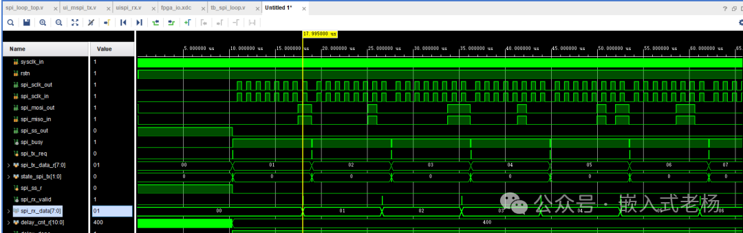
The system clock sysclk_in outputs stably at 100MHz (period 10ns), the SPI clock spi_sclk_out is at 1MHz (100 division) and is low when idle (consistent with CPOL=0); spi_ss_out is pulled low before sending (selecting the slave device), remains low during the transmission of 8 bits of data, and is immediately pulled high after sending, with no glitches in timing; spi_mosi_out outputs incrementing serial data, and after receiving through the loopback, the parallel data output from spi_rx_data_out is completely consistent with the sent data, with spi_rx_valid_out set high for one clock cycle at the end of each byte reception.