How to Optimize Complex Multiplication Operations in FPGA Development?
In FPGA digital signal processing, such as in the baseband processing of wireless communication systems, complex multiplication is frequently used. How can we optimize complex multiplication? We will start from the basic principles and gradually consider optimization strategies for complex multiplication.
First, let’s review the formula for complex multiplication. Given two complex numbers: a + bi and c + di, their product is:
It can be seen that a direct implementation of complex multiplication requires 4 multiplications and 2 additions/subtractions. By directly implementing according to the above formula, each clock cycle computes one complex multiplication, using 4 DSP Slices (multipliers) in the FPGA, and the combination delay of the multipliers and adders will also be relatively large.
How to optimize while reducing DSP resource usage and lowering logic delay?
Using an algorithm that optimizes with 3 multipliers is a classic mathematical optimization. By cleverly combining additions and subtractions, the number of multiplications can be reduced from 4 to 3. The calculation process is as follows:
First, calculate three intermediate products:
Then, the real and imaginary parts can be obtained from these intermediate values:
The advantage of this approach is that it saves 1 DSP Slice, which is significant for large-scale complex multiplication, but it increases the logic of the adders and the final calculations, with a longer adder chain on the imaginary path, which may slightly increase logic delay.
Using a pipelined processing structure with 3 multipliers, inserting registers between longer combinational logic paths (such as an adder following a multiplier) divides it into multiple shorter clock cycle stages, the pipelined processing of the 3 multipliers is as follows:
- First stage: Pre-addition and calculation
- Second stage: 3 parallel MULTs (multipliers)
- Third stage: Calculation
After pipelining, each stage has a shorter combinational logic path, making it easier for timing convergence, allowing it to run at a higher clock frequency.
Modern FPGA DSP Slices are not just multipliers; they also integrate pre-adders, post-adders, and accumulators, which can be utilized to efficiently implement the aforementioned 3 multiplier structure. For example, the Xilinx DSP48E1 Slice can be configured in a mode suitable for calculating a + bi
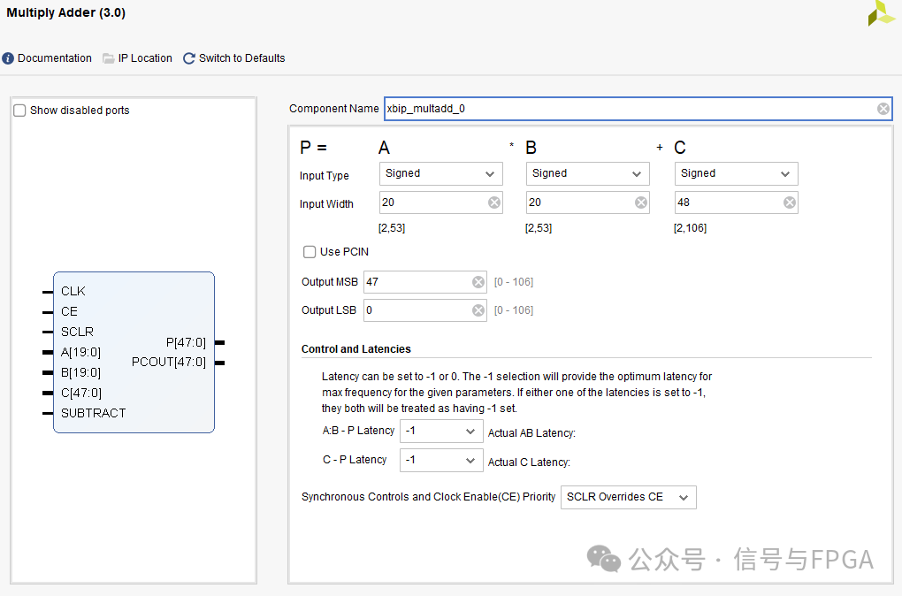
Considerations for Optimization Strategies
| Scheme | Advantages | Disadvantages | Applicable Scenarios |
|---|---|---|---|
| Direct Implementation (4 Multiplications) | Simple structure, lowest delay, high accuracy | Most DSP resource consumption | Scenarios that are extremely sensitive to delay and have abundant DSP resources |
| 3 Multipliers, Pipelined Processing | Greatly increases clock frequency and throughput | Increased register resources | Almost all high-performance computing scenarios |
In general, the preferred method is the 3 multiplier structure with pipelined processing, which enhances system performance.