“My design runs at 200MHz, isn’t that impressive?”
Brother, you might be asking the wrong question. In the high-performance world of FPGAs, a high clock frequency does not necessarily equate to good system performance.
You have surely encountered designs running at 200MHz that take 10ms to process a frame of image, while a carefully designed 150MHz system might only take 5ms. Why? Because you need to establish a systematic performance trade-off framework.
01
Three Dimensions of Performance and Quantification Methods
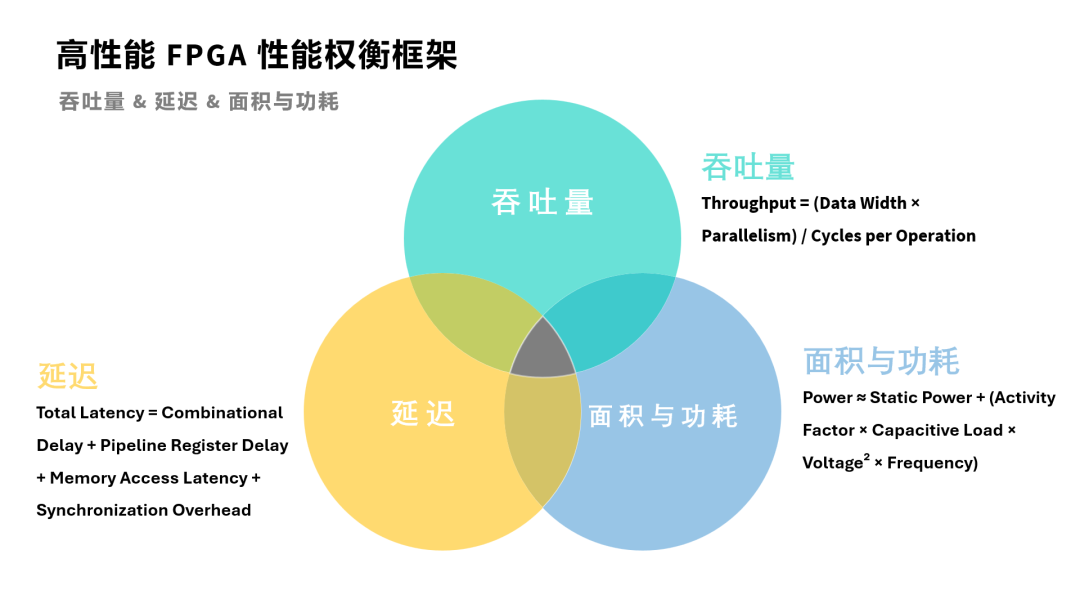
To establish a quantitative performance analysis mindset, one must first understand the essence of three core dimensions and their interdependent relationships.
1
Throughput
Throughput is the total workload per unit time, quantifying your system’s efficiency. The theoretical model for throughput can be simplified as:Throughput = (Data Width × Parallelism) / Cycles per Operation
Increasing throughput is not solely about raising frequency; increasing data width and parallelism are often effective means as well.
• Video transcoding servers: The core metric is “how many frames are transcoded per second.” Typically, multiple parallel encoding pipelines are packed into the FPGA to work simultaneously—this is trading area for throughput.
• Network switch chips: The core metric is “how many data packets are forwarded per second.” We design deep pipelines to ensure that data can be “ingested” and “output” every clock cycle, pursuing uninterrupted port performance.
• Data center accelerator cards: Throughput is usually enhanced by increasing the number of parallel computing units.
2
Latency
Latency is the time taken for data to move from input to output, defining your system’s response speed. The total latency can be broken down as:Total Latency = Combinational Delay + Pipeline Register Delay + Memory Access Latency + Synchronization Overhead
• ADAS brake control: From radar detecting an obstacle to issuing a brake signal, it typically needs to reach millisecond or even microsecond levels. The logic here must be extremely simple, and the path must be the shortest, with stringent latency requirements. In these scenarios, optimizing data paths, reducing unnecessary pipeline stages, and choosing low-latency memory access methods are crucial.
• High-frequency trading systems: To be faster than competitors by a few microseconds, the entire processing path must be “straightforward,” minimizing any buffering. In finance, latency is money.
3
Area and Power Consumption
The trade-off between area and power consumption can be likened to a complex puzzle. Area and power consumption are tightly coupled, and their relationship can be approximated as:Power ≈ Static Power + (Activity Factor × Capacitive Load × Voltage² × Frequency)
Dynamic power consumption is proportional to the square of the voltage. Therefore, in scenarios such as mobile devices (like AR/VR glasses) or large-scale data centers, low-power design is a core consideration. Reducing area through logic reuse not only lowers static power but can also significantly reduce dynamic power by decreasing wiring capacitance, achieving super-linear benefits.
• Large-scale AI inference cards: A server may house dozens of cards, and if each card’s resources are over-utilized, heat dissipation and yield become problematic. Area must be strictly controlled; otherwise, total costs cannot be sustained.
• Data centers: Electricity costs are a major expense. A 10% reduction in design power consumption can save several million yuan annually for a data center operating 100,000 FPGAs.
• Cost-sensitive smart appliances: The goal is to use the cheapest FPGA with the least resources. Engineers need to optimize code and reuse logic, such as allowing a multiplier to be used by multiple modules at different times.
• Area-sensitive electronic products: For electronic products like AR/VR glasses, the battery size is limited, and “sleeping when possible” is the first principle. Engineers must use techniques like clock gating to turn off most logic clocks when the user is not interacting.
Discussing optimization without specific requirements is just nonsense. An excellent architect begins to sketch this trade-off map in their mind the moment they receive the requirements. The three dimensions mentioned above are often contradictory and interdependent. A skilled architect needs to balance these factors based on the application scenario.

• Want to maximize throughput? Use more parallelism and pipelining, but this will increase area and power consumption.
• Want to minimize latency? Reduce processing stages, but this will limit frequency and throughput.
• Want the smallest area? Resource reuse and serial operation, but this will sacrifice throughput.
• Want the lowest power consumption? You need to lower frequency and reduce switching rates, but this may directly impact performance.
02
Dialogue with AI Technology Leaders
“Take a step back, move two steps forward”
The high-performance trade-off thinking discussed in this article, which balances throughput, latency, area, and power consumption, is not only applicable to FPGAs; it is actually a common language in all chip design.
Recently at the ICCAD-expo, I participated in a closed-door communication meeting where the product director of Arm China shared his design philosophy in the field of edge AI chips. You might find it enlightening:
In the field of edge AI chips (such as NPUs), the design focus has shifted from the extreme pursuit of “area efficiency” and “energy efficiency” to how to quickly deploy cloud algorithms to the edge. Given the current lack of revolutionary breakthroughs in battery technology, edge computing power is strictly limited to a few watts.
Within the limited power and area budget, designers even need to consider “taking a step back” and relaxing the pursuit of certain traditional extreme metrics (such as extreme area efficiency and energy efficiency) in exchange for better connectivity and versatility—specifically, enhancing processing performance through compilation optimization and improved Tensor computation capabilities while retaining necessary Vector general-purpose processing units, thus finding the optimal balance between “dedicated” and “general-purpose” for specific scenarios.
Performance optimization begins with correct understanding.The essence of high-performance chip design has never been about blindly chasing clock frequency, but rather establishing a systematic trade-off mindset centered on throughput, latency, area, and power consumption.In summary: Understand the scenario, then make trade-offs.