Follow+Star Public Account Number, don’t miss out on exciting contentSource | Hardware Notebook
Hello everyone, today we will discuss in detail the SPI interface. The article is a bit lengthy, so it is recommended to bookmark it and read it slowly.
SPI has now become the most commonly used communication method between MCUs and peripheral devices. It is a synchronous, full-duplex, master-slave communication interface. The working principle is quite straightforward: the master generates a clock signal, and the slave synchronously sends and receives data according to this clock. It allows for bidirectional transmission, enabling data exchange between master and slave devices within the same clock cycle.
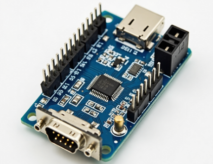
This design makes SPI both simple and efficient, especially suitable for scenarios requiring fast data transmission. However, it is important to note that SPI does not have a standard communication protocol, and devices from different manufacturers may have differences, so it is essential to carefully read the chip manual when using it.
011
Typical Application Scenarios
The core advantages of the SPI interface lie in its simplicity and flexibility, with typical application scenarios including:
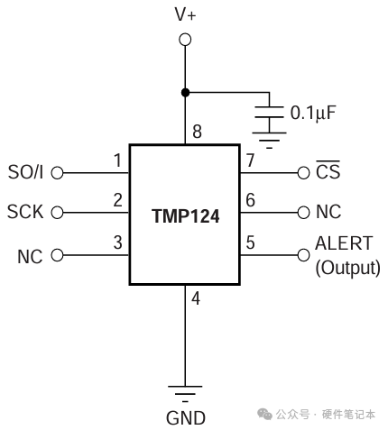
1. Sensor data acquisition (such as temperature sensors, IMUs), for example: the TMP124 chip, which is an industrial-grade digital temperature sensor launched by TI, featuring high precision + SPI interface combination, suitable for scenarios with stringent temperature measurement requirements.
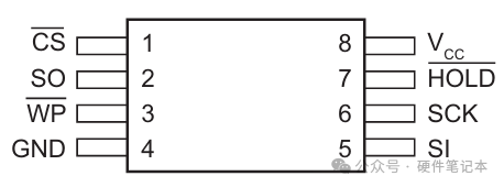
2. Memory read/write (Flash, EEPROM), for example, the small-capacity AT25040, which is commonly used to store configuration parameters and calibration data.
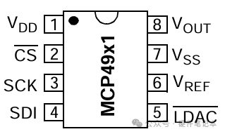
3. Digital signal conversion (ADC/DAC). For example, the general-purpose ADC chip MCP4921, which is a low-cost 12-bit digital-to-analog converter (DAC) launched by Microchip, featuring ease of use + SPI interface combination, suitable for scenarios requiring digital control of analog output.
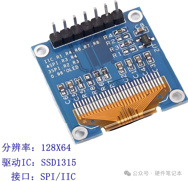
4. Display driving (OLED, TFT screens), for example, the commonly used 0.96-inch OLED screen, which generally has both I2C and SPI interfaces. Although SPI occupies two IO ports, it is much faster than I2C.
021
SPI Connection Methods and Operating Speeds
Connection Methods
The SPI interface can be either 3-wire or 4-wire; here we mainly introduce the commonly used 4-wire SPI interface, which has four signals:
-
Chip Select (CS): Chip select signal, active low
- Clock (SPI CLK, SCLK): Clock signal generated by the master
- MOSI: Master output, slave input
- MISO: Master input, slave output
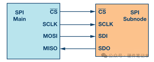 SPI connection between master and slave It is important to note the wiring of MOSI and MISO between the master and slave, which is different from serial TX and RX; many people easily get it wrong. The master’s MISO connects to the slave’s MISO, and the master’s MOSI connects to the slave’s MOSI,directly connected without crossing. How to determine which is the master? The device that generates the clock signal is called the master. The data transmitted between the master and slave is synchronized with the clock generated by the master. Additionally, there can only be one master in the SPI interface, but there can be one or more slaves. The chip select signal from the master is used to select the slave. This is usually an active low signal, and when pulled high, the slave is disconnected from the SPI bus. When using multiple slaves, the master needs to provide a separate chip select signal for each slave.
Operating Speeds
The typical range of SPI speeds is: 1 MHz to 100 MHz (4 Mbps to 400 Mbps), with specific rates depending on the device grade:
Consumer-grade ICs: 1-10 MHz (4-40 Mbps)Industrial-grade devices: 10-25 MHz (40-100 Mbps) However, in practical applications, we are limited by peripheral support (e.g., Flash chips can reach 80 MHz, while sensors typically operate at 8 MHz).
By comparison, the speed of I2C is much lower: Standard mode 100 Kbps, high-speed mode 5 Mbps (theoretical value), but I2C occupies two fewer IO ports, so I2C wins in pin efficiency, while SPI wins in speed.
031
Data Transmission
The data transmission in SPI proceeds as follows:
First, the controlling device must generate a clock signal (SCLK), which acts as the metronome for communication. At the same time, the master must pull the chip select signal (CS) low to select the slave device for communication; this CS signal is usually active low, so the master must provide it with a logic 0.
The most powerful aspect of SPI is that it is full-duplex, meaning the master can send data out via the MOSI line while the slave can also send data back to the master via the MISO line simultaneously. Specifically, the master sends data bit by bit onto the MOSI line while simultaneously receiving data bit by bit on the MISO line.
All of this data transmission and reception strictly follows the edges of the clock signal, and you can choose to sample the data on the rising or falling edge of the clock. As for how many bits of data to transmit in each communication, this depends on the specifications of the specific device, as different chips may have different requirements.
Let’s look at two animations
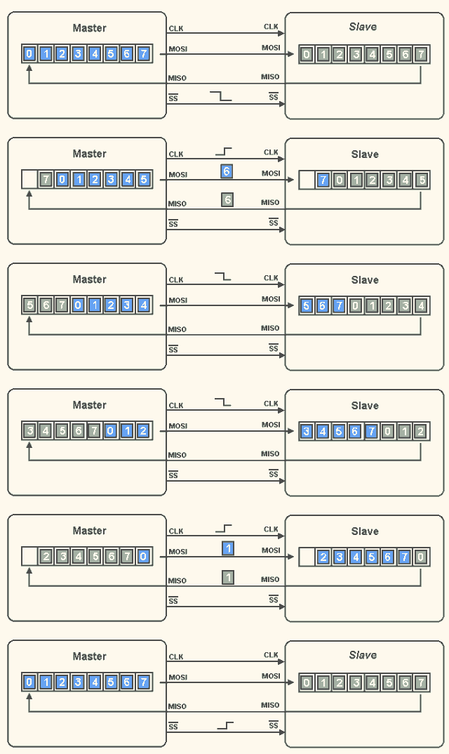
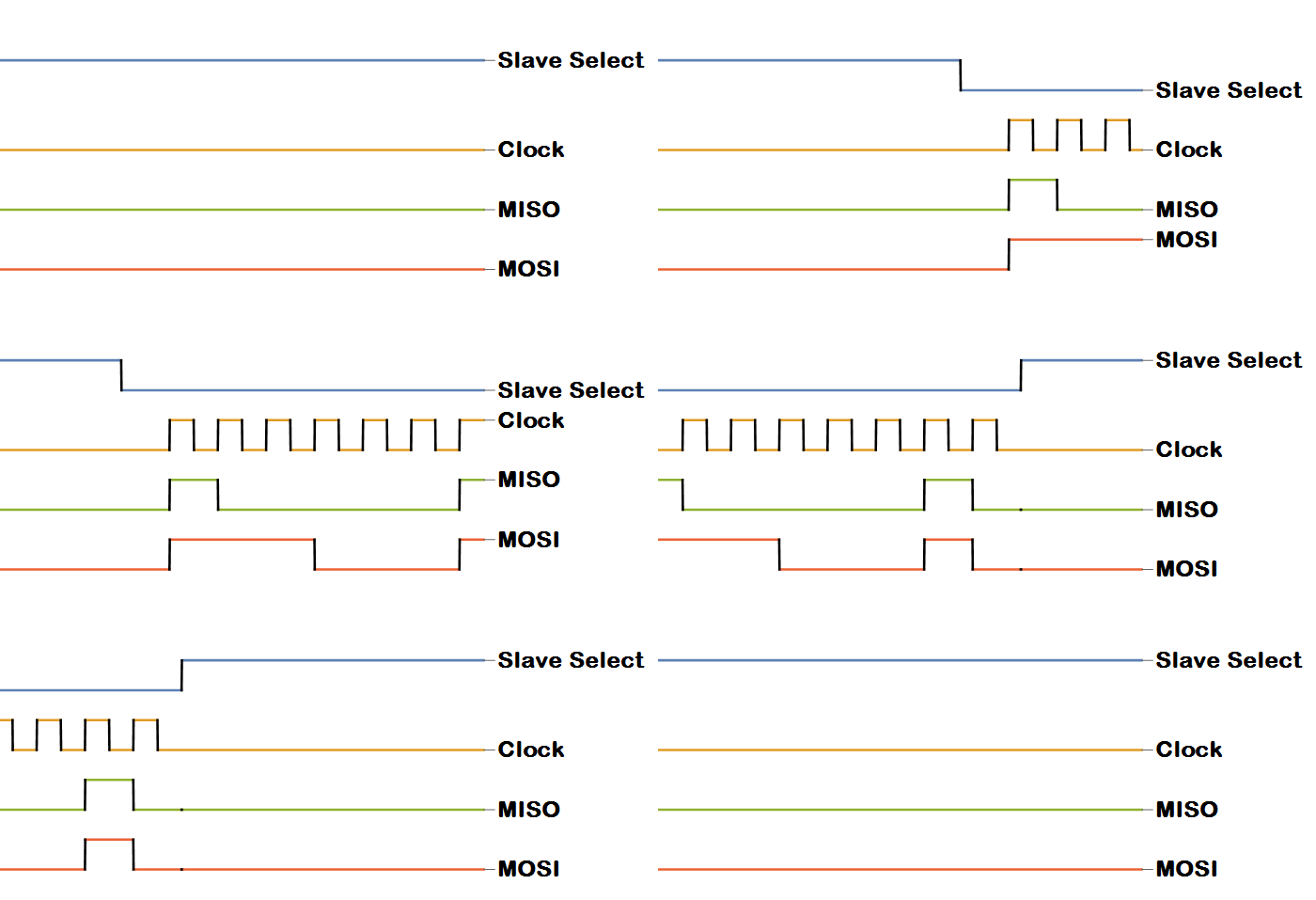
During this process, three points must be noted:
1. The clock must be generated by the master;
2. The CS signal must be pulled low in advance to select the slave;
3. Data transmission and reception occur simultaneously, not one after the other. This design makes SPI both simple and efficient, especially suitable for scenarios requiring fast data transmission.
041
Operating Modes
There are 4 operating modes for SPI, mainly configured through the CPOL and CPHA parameters:
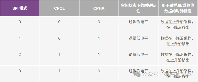
Below is the timing diagram for SPI mode 0.
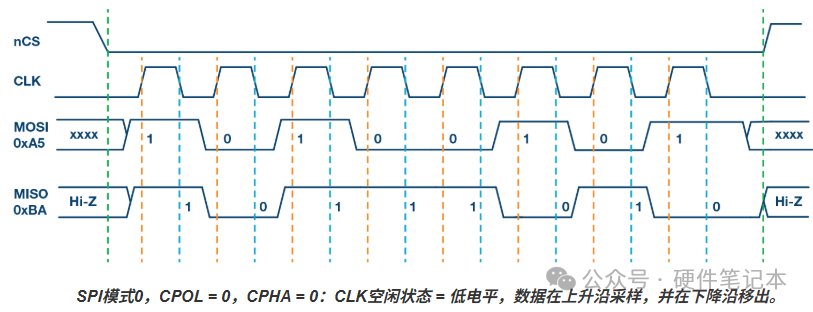
Below is the timing diagram for SPI mode 0.
The start and end of the transmission are indicated by green dashed lines; the sampling edge is indicated by orange dashed lines; the shifting edge is indicated by blue dashed lines. Of course, these diagrams are for reference only. To successfully perform SPI communication, it is essential to refer to the device’s datasheet and ensure compliance with the device’s timing specifications.
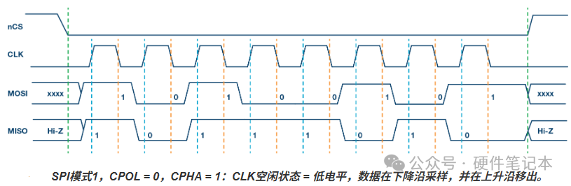
Below is the timing diagram for SPI mode 1. At this time:
The clock polarity is 0, indicating that the idle state of the clock signal is low;
The clock phase is 1, indicating that data is sampled on the falling edge (as shown by the orange dashed line), and data is shifted out on the rising edge of the clock signal (as shown by the blue dashed line).
Below is the timing diagram for SPI mode 1. At this time:
The clock polarity is 0, indicating that the idle state of the clock signal is low;
The clock phase is 1, indicating that data is sampled on the falling edge (as shown by the orange dashed line), and data is shifted out on the rising edge of the clock signal (as shown by the blue dashed line).
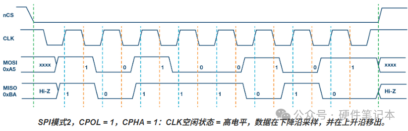
Below is the timing diagram for SPI mode 2. At this time:
The clock polarity is 1, indicating that the idle state of the clock signal is high.
The clock phase is 1, indicating that data is sampled on the falling edge (as shown by the orange dashed line), and data is shifted out on the rising edge of the clock signal (as shown by the blue dashed line).
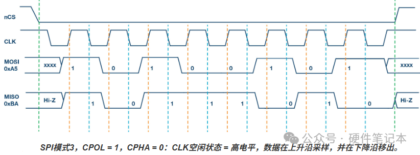
Below is the timing diagram for SPI mode 3. At this time:
The clock polarity is 1, indicating that the idle state of the clock signal is high.
The clock phase is 0, indicating that data is sampled on the rising edge (as shown by the orange dashed line), and data is shifted out on the falling edge of the clock signal (as shown by the blue dashed line).
Below is the timing diagram for SPI mode 3. At this time:
The clock polarity is 1, indicating that the idle state of the clock signal is high.
The clock phase is 0, indicating that data is sampled on the rising edge (as shown by the orange dashed line), and data is shifted out on the falling edge of the clock signal (as shown by the blue dashed line).
051
Multi-Slave Configuration
We can use multiple slaves with a single SPI master. Slaves can be connected in conventional mode or in daisy chain mode.
Conventional SPI Mode:
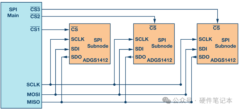
In our conventional SPI connection mode, the master must provide a separate chip select signal line (CS) for each slave device. When the master pulls the CS signal of a specific slave low, that slave is selected, and at this point, the clock and data signals on the MOSI and MISO lines can communicate with that specific slave. Follow the public account: Hardware Notebook
There is an important limitation: only one slave’s CS signal can be pulled low at a time; if multiple CS signals are pulled low simultaneously, it will cause multiple slaves to return data on the MISO line at the same time, resulting in data conflicts, and the master will not be able to distinguish which data comes from which slave.
As the number of slaves connected to the system increases, the number of chip select lines the master needs to provide will also increase accordingly. For example, connecting 8 slaves requires 8 separate CS lines, which quickly occupies the master’s IO port resources, thus limiting the number of slaves the system can support. To solve this problem, some expansion techniques can be used, such as using multiplexers (MUX) to generate chip select signals. However, this solution will increase some hardware complexity, requiring additional multiplexer chips.
Daisy Chain Mode:
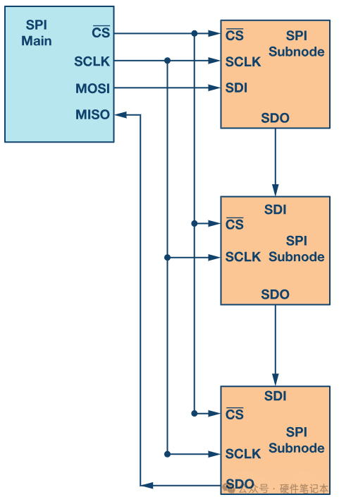
In the SPI daisy chain connection mode, all slave devices share the same chip select signal (CS), propagating from one slave to the next. The specific working process is: after the master issues the clock signal (SCLK), data is first transmitted to the first slave, and the first slave provides the data to the second slave, and so on. All slaves use the same clock signal for synchronization.
This connection method is characterized by requiring more clock cycles for data transmission. For example, in an 8-bit data width system, if we want the third slave to receive data, it requires 24 clock pulses (3 slaves × 8 bits), while in conventional SPI mode, it only requires 8 clock pulses. This is because the data needs to pass through each slave in sequence, and each slave will process and forward the data.
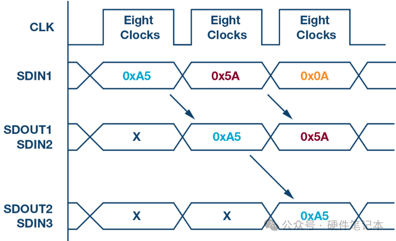
Daisy Chain Configuration: Data Propagation
It is important to note that not all SPI devices support daisy chain mode. Before using this connection method, it is essential to carefully check the technical manual of the chips used to confirm whether they support daisy chain functionality. Some chips may only support the conventional independent chip select mode. Additionally, while daisy chain mode saves chip select signal lines, it reduces communication efficiency, so it is necessary to weigh the choice based on actual application needs.
061
Summary
Although the SPI interface is simple, there are many details to pay attention to in practical applications:
1. Wiring must be correct (directly connected, not crossed);
2. Modes must match (refer to the device manual);
3. When using multiple slaves, choose the connection method wisely.
Remember these key points, and you will be able to use the SPI interface effectively! If you encounter problems, the most reliable method is to consult the device’s datasheet.
If this article has been helpful to you, don’t forget to like, bookmark, and share it with more people in need!
———— END ————
RT-Trace domestic debugging tool + RT-Thread greatly improves development efficiency!
Development tool! Onboard Raspberry Pi GPIO interface makes testing chip performance easier
MCU high performance + AI will be the trend of the future!