
Click the blue text
Follow us
1. Introduction to W25Q64
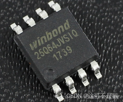
The W25Q64 (64Mbit) is a serial FLASH memory solution designed to provide minimal space, pin count, and power consumption for systems. The 25Q series offers greater flexibility and superior performance compared to standard serial FLASH memory. Based on double/quad SPI, they can immediately provide data to RAM, including sound, text, and data.
The W25Q64 consists of pages of 256 bytes, which can be programmed in one page programming command. It can erase 16 pages (one sector), 128 pages (32KB block), 256 pages (64KB block), and perform a full chip erase at once.
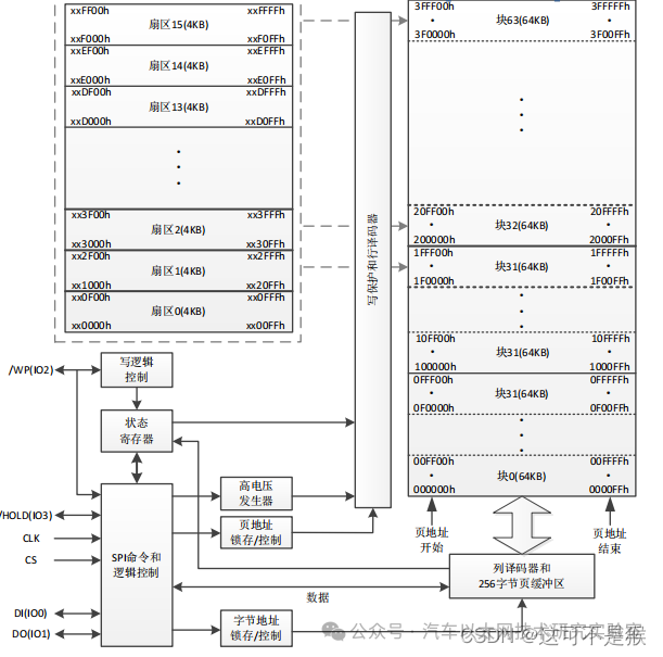
The memory structure of W25Q64: one page of 256 bytes, 4k (4096 bytes) per sector, 16 sectors per block, with a total capacity of 8M bytes, comprising 128 blocks and 2048 sectors. The SPI supports a maximum of 80MHz, and when using fast read double/quad commands, it achieves a maximum rate of 160MHz for double output and 320MHz for quad output.
Features:
-
Standard, double, and quad SPI
-
High-performance serial FLASH memory
-
Flexible 4KB sector structure
Unified sector erase and block erase, programming 256 bytes at once, with at least 100,000 write/erase cycles, and data retention for 20 years.
-
Advanced security features
-
Low power consumption, wide temperature range
Single power supply of 2.7~3.6V, operating current of 4mA, and operational temperature range of -40℃ to 85℃.
Package
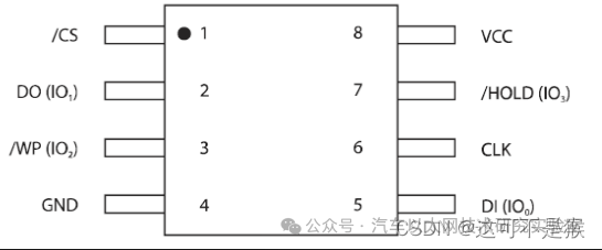
8Pin SOIC 208-mil
Pin Description
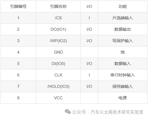
1.1 Chip Select (/CS)
The SPI chip select (/CS) pin enables and disables chip operation. When /CS is high, the chip is not selected, and the serial data output (IOx) pin is in a high-impedance state, with the chip in a low-power standby state unless it is internally erasing. When /CS goes low, the chip’s power consumption increases to normal operation, allowing data to be read from and written to the chip. After power-up, /CS must transition from high to low before receiving new commands.
1.2 Serial Data Input/Output (DI, DO)
Standard SPI transmission uses the unidirectional DI (input) pin to continuously write commands, addresses, or data into the chip on the rising edge of the serial clock (CLK). The standard SPI uses the unidirectional DO (output) pin to read data or status from the chip on the falling edge of CLK.
1.3 Write Protect (/WP)
The write protect pin (/WP) is used to protect the status register. The block protection bits (SEC, TB, BP2, BP1, and BP0) in the status register and the status register protection bit (SRP) provide partial or full hardware protection for the memory. The /WP pin is active low. When the QE bit of status register 2 is set, the function of the /WP pin (hardware write protection) is disabled and used as IO2.
1.4 Hold Pin (/HOLD)
When the /HOLD pin is active, it allows the chip to pause operation. When /CS is low, if /HOLD goes low, the DO pin will become high-impedance, and signals on the DI and CLK pins will be invalid. When /HOLD goes high, the chip resumes operation. The /HOLD function is used when multiple devices share the same SPI bus. The /HOLD pin is active low. When the QE bit of status register 2 is set, the function of the /HOLD pin is disabled and used as IO3.
1.5 Serial Clock (CLK)
The serial clock input pin provides timing for serial input and output operations. Device data transmission starts from the most significant bit, with a data transmission format of 8 bits, and data sampling begins on the rising edge.
1.6 Structural Block Diagram
1.7 SPI Operation
The W25Q64/16/32 compatible SPI bus includes four signals: serial clock (CLK), chip select (/CS), serial data input (DI), and serial data output (DO). Standard SPI uses the DI input pin to continuously write commands, addresses, or data into the chip on the rising edge of CLK. The DO output reads data or status from the chip on the falling edge of CLK.
It supports SPI bus operating modes 0 (0,0) and 3 (1,1). The main difference between modes 0 and 3 is the idle state of the CLK signal; when the SPI master is ready, but data has not yet been transmitted to the serial Flash, the idle state of the CLK signal is low for mode 0.
Device data transmission starts from the most significant bit, with a data transmission format of 8 bits, and data sampling begins on the second clock edge, with the clock line CLK being high in the idle state.
1.8 Status Register

The status register of the W25Q64 supports read and write operations, with read status register (command: 05H) and write status register (command: 01H).
S0: Busy Bit (BUSY). The BUSY bit is a read-only bit. When the device is executing “page programming”, “sector erase”, “block erase”, “chip erase”, or “write status register” commands, this bit is automatically set. At this time, all commands except for the “read status register” command are ignored. After the programming, erasing, and writing status register commands are completed, this bit automatically resets to 0, indicating that the chip can accept other commands.
S1: Write Enable Bit (WEL). The WEL bit is a read-only bit located in S1 of the status register. It is set when the “write enable” command is executed. When the chip is in “write protect state”, this bit is 0. The following two conditions will enter the “write protect state”:
-
After power loss.
-
After executing the following commands: write disable, page programming, sector erase, block erase, chip erase, and write status register.
Other status bits: omitted.
2. Pin Connections
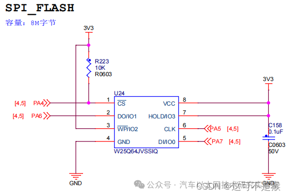
Note: This schematic is from the Wildfire Dominator development board.
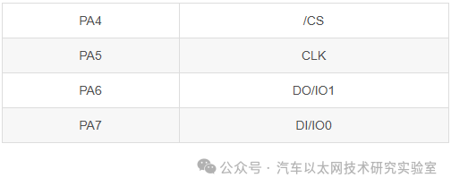
3. SPI
3.1 Hardware SPI
The MCU used in this instance is STM32F103ZET6. For detailed information on hardware SPI, please refer to the STM32F10x user manual.
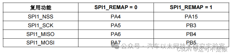
SPI1 Multiplexing Function Remapping
When using the MCU hardware SPI, it is necessary to select the appropriate IO ports and enable the AFIO peripheral.
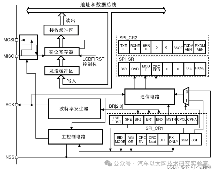
SPI Block Diagram
Typically, SPI connects to external devices via four pins:
-
MISO: Master In/Slave Out. Sends data in slave mode and receives data in master mode.
-
MOSI: Master Out/Slave In. Receives data in slave mode and sends data in master mode.
-
SCK: Serial Clock, output from the master device and input to the slave device.
-
NSS: Slave Select (Chip Select Pin).
In this usage, SPI1 should be set as the master device to control the W25Q64.
3.1.1 Clock Polarity and Clock Phase
The CPOL and CPHA bits in the SPI_CR register can be combined to form four possible timing relationships. CPOL (Clock Polarity) controls the idle state level of the clock when no data is being transmitted: when CPOL=0, the idle clock level is low; when CPOL=1, the idle clock level is high. CPHA (Clock Phase) controls at which clock edge data is latched: when CPHA=0, data is latched on the first clock edge; when CPHA=1, data is latched on the second clock edge. The clock phase must be used in conjunction with the clock polarity to determine at which clock edge data is latched.
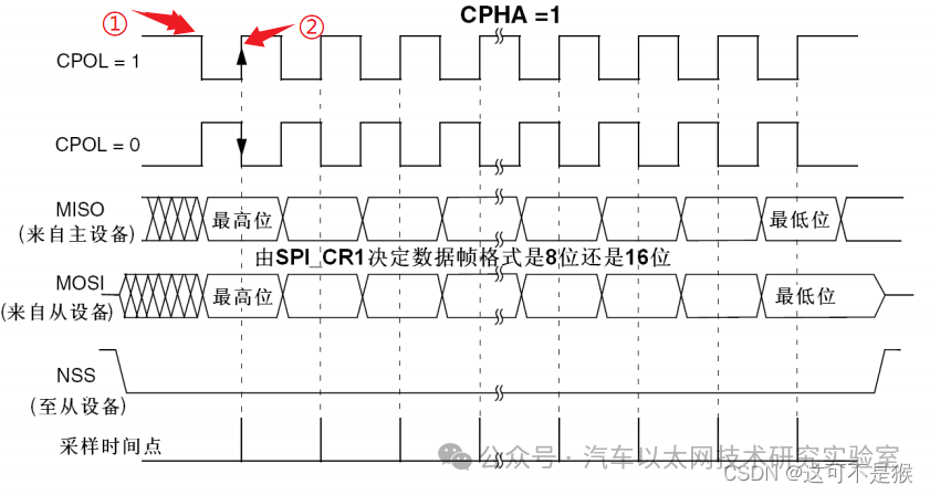
CPHA=1
As shown in the figure above, the clock phase is 1, meaning data is latched on the second clock edge.
When the clock polarity (CPOL) is 1, the idle level of CLK is high, the first edge is falling, and the second edge is rising. Data is latched on the rising edge of CLK. The master device can send data to the slave device when the clock is low and read data when the clock is high (simulated SPI concept).
When the clock polarity (CPOL) is 0, the idle level of CLK is low, the first edge is rising, and the second edge is falling. Data is latched on the falling edge of CLK. The master device can send data to the slave device when the clock is high and read data when the clock is low (simulated SPI concept).
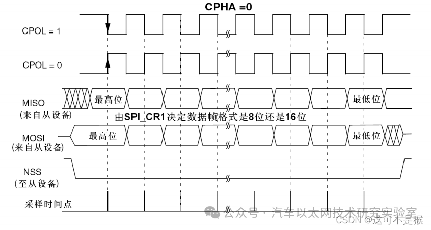
CPHA=0
When the clock phase is 0, data is latched on the first clock edge.
When the clock polarity (CPOL) is 1, the idle level of CLK is high, the first edge is falling. Data is latched on the falling edge of CLK. The master device can send data to the slave device when the clock is high and read data when the clock is low (simulated SPI concept).
When the clock polarity (CPOL) is 0, the idle level of CLK is low, the first edge is rising. Data is latched on the rising edge of CLK. The master device can send data to the slave device when the clock is low and read data when the clock is high (simulated SPI concept).
3.1.2 Data Frame Format
According to the LSBFIRST bit in the SPI_CR1 register, the output data bits can be either MSB (most significant bit) first or LSB (least significant bit) first.
According to the DFF bit in the SPI_CR1 register, each data frame can be 8 bits or 16 bits. The selected data frame format applies to both sending and receiving.
3.1.3 Configuring as SPI Master Mode
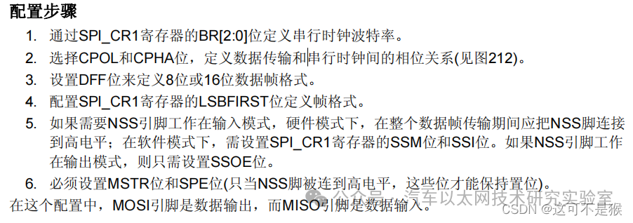
Register Development Mode
As shown in the figure above, the official register configuration method mainly configures the baud rate for SPI data transmission speed; clock polarity and clock phase; frame format (8-bit or 16-bit, MSB first or LSB first); chip select pin working mode, etc. To reduce the time spent looking up registers in the manual, this instance uses the firmware library to configure SPI.
API: void SPI_Init(SPI_TypeDef* SPIx, SPI_InitTypeDef* SPI_InitStruct)
Initializes the SPI peripheral.
SPI_InitTypeDef Initialization structure
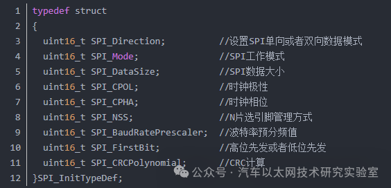
(1) SPI_Direction sets the SPI data mode to unidirectional or bidirectional.
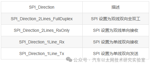
(2) SPI_Mode sets the SPI operating mode. Master SPI (SPI_Mode_Master), Slave SPI (SPI_Mode_Slave).
(3) SPI_DataSize sets the size of the SPI data. 16-bit data frame structure (SPI_DataSize_16b), 8-bit data frame structure (SPI sends and receives 8-bit frame structure).
(4) SPI_CPOL sets the idle clock level. Idle clock high (SPI_CPOL_High), idle clock low (SPI_CPOL_Low).
(5) SPI_CPHA sets the clock edge at which data is captured. Data is captured on the first edge (SPI_CPHA_1Edge), data is captured on the second edge (SPI_CPHA_2Edge).
(6) SPI_NSS specifies whether the NSS signal is managed by hardware (NSS pin) or software (using the SSI bit). NSS is managed by hardware (SPI_NSS_Hard), internal NSS signal is controlled by software (SPI_NSS_Soft).
(7) SPI_BaudRatePrescaler defines the value for the baud rate prescaler, which is used to set the SCK clock for sending and receiving.
(8) SPI_FirstBit specifies whether data transmission starts from the MSB or LSB. Data transmission starts from the MSB (SPI_FisrtBit_MSB), data transmission starts from the LSB (SPI_FisrtBit_LSB).
(9) SPI_CRCPolynomial defines the polynomial used for CRC value calculation.
3.1.4 SPI Initialization Configuration
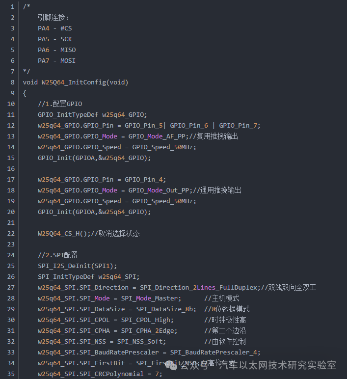

(1) Configure GPIO working mode. CS is controlled by the IO pin, configured as a general-purpose push-pull output mode; the other three pins are controlled by SPI1, configured as multiplexed push-pull output mode.
(2) Configure SPI. Before configuring SPI, the chip select pin can be pulled high.
Since data needs to be read and written, it is configured as master mode, full-duplex data mode.
Data frame format is configured for 8-bit data with MSB first.
Clock polarity and clock phase can be configured for mode (0,3), here configured for mode 3, with clock polarity high and clock phase capturing on the second edge.
The chip select pin is controlled by software. (Hardware control: SPI control)
Clock division is chosen as 4. Other division values can also be used.
(3) Enable SPI1.
Note: Peripheral clock is configured in main.c.
3.15 Read/Write Data Functions
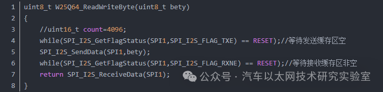
(1) Wait for the transmitter to be empty; a delay can be added here to avoid program hang. Data can only be sent when there is no data in the transmitter register.
(2) Wait for the receiver buffer to have data before receiving data.
3.2 Simulated SPI
Compared to hardware SPI, simulated SPI does not require the MCU to have the SPI peripheral; it can use ordinary IO ports to simulate SPI timing for communication.
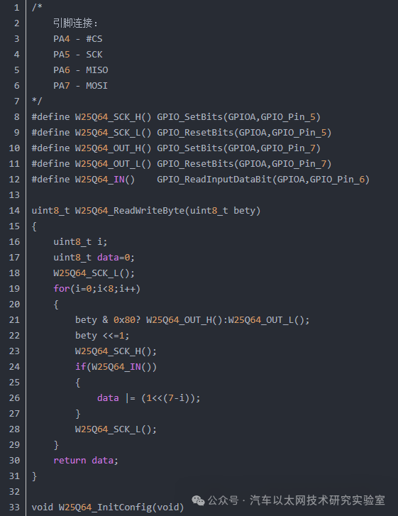
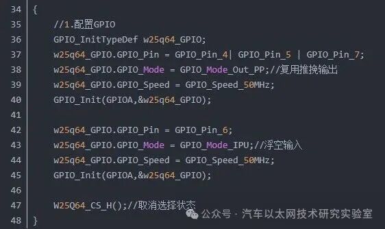
(1) Configure GPIO working mode; /CS, CLK, and MOSI pins are configured as output mode, and MISO is configured as input mode.
(2) Write the simulated SPI function. In using simulated SPI, mode 0 is selected, with clock polarity 0 and clock phase 0. The idle level of the clock is low, and data is captured on the rising edge.
-
Define an unsigned char variable data to store the received data.
-
Pull the clock pin low.
-
In a for loop, iterate 8 times to read or send one byte.
-
On the rising edge, capture data, so the clock pin should output high or low while keeping stable before the rising edge arrives. Here, a ternary operator is used to get the highest bit of the byte to be sent, and the lower bit is shifted to the highest bit for the next bit transmission.
-
Pull the clock pin high.
-
When the clock pin is high, read data and shift it to the corresponding bit.
-
Pull the clock low to prepare for the next rising edge, or keep the clock high after the last bit of data transmission is complete.
4. W25Q64
4.1 Read W25Q64 Manufacturer/Device ID (90H)
Before reading and writing FLASH, the manufacturer/device ID of W25Q64 can be read to verify if the SPI read/write function is operational.
First, pull the /CS pin low, then send the command 90H through the function W25Q64_ReadWriteByte to the chip, followed by sending the 24-bit address 000000H to the chip. The chip will then send the “Manufacturer ID” and “Device ID” on the DO pin on the rising edge, which can be read using the W25Q64_ReadWriteByte function.
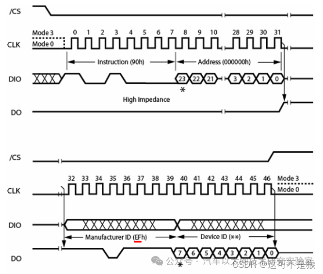
Reading Manufacturer/Device ID Timing
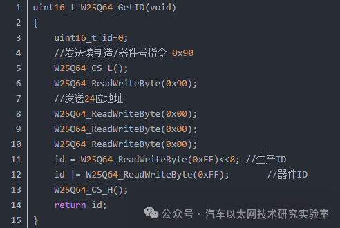
(1) Pull the chip select line low.
(2) Send the read “Manufacturer/Device ID” command 90H, and send the 24-bit address 000000H.
(3) Read the Manufacturer ID and Device ID.
(4) After reading, pull the chip select high.
Manufacturer ID=0xEF, Device ID=0x16.
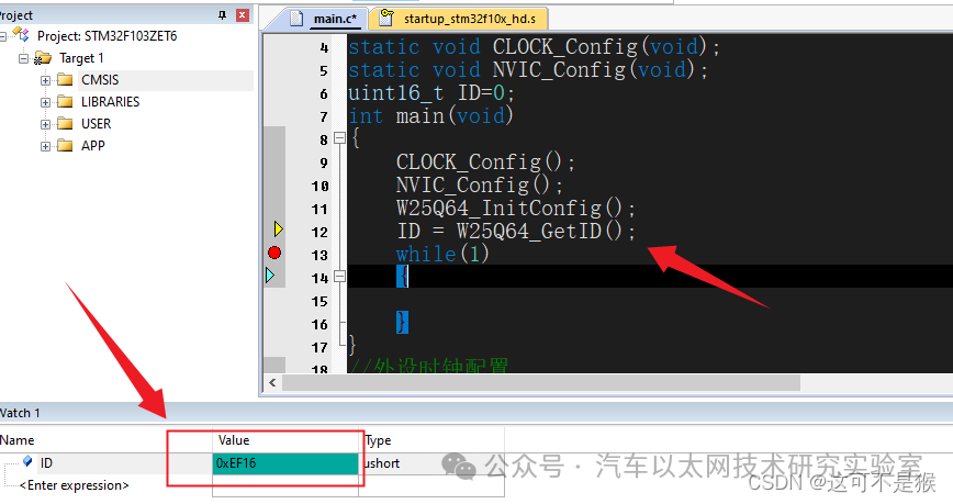
Error: When using hardware SPI, the mode (0,3) reads the ID and sends/receives data the same as in simulated SPI mode 0. When using simulated SPI mode 3, data transmission works normally, but there will be discrepancies in the ID number read. Friends learning from this article can try simulated SPI mode 3 to see if this issue occurs.
4.2 Write Enable (06H)
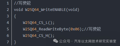
The write enable command will set the WEL bit in the status register. Before executing each “page programming”, “sector erase”, “block erase”, “chip erase”, and “write status register” command, WEL must be set. Pull /CS low, send the 06H command to the chip, and then pull the /CS pin high.
4.3 Erase Command
Before writing data to FLASH, it must be ensured that the memory is empty, and the erased sector bits are all 1, with sector bytes all being FFH.
4.3.1 Sector Erase (20H)
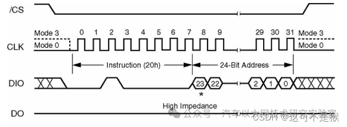
The sector erase command will erase one sector (16 pages, 4096 bytes). Before executing the sector erase command, the “write enable” command must be executed to ensure that the WEL bit is 1.
First, pull the /CS pin low, then send the 20H command to the chip, followed by sending the 24-bit sector address to the chip, and then pull the /CS high. If /CS is not pulled high in time, the command will not take effect. During the execution of the command, the BUSY bit is 1. After the command is completed, BUSY will reset, and WEL will also reset.
Sector Erase Timing
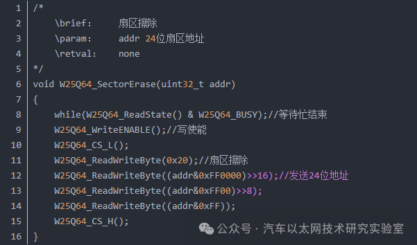
(1) When continuously erasing sectors, there may be a situation where the previous sector’s code execution has ended but the erase has not finished, so it is necessary to wait for the erase to complete. Here, I use a busy wait, but a timeout can be added.
(2) Write enable, ensuring that the WEL bit is 1 before erasing the sector.
(3) Pull the chip select low.
(4) Send the sector erase command and the 24-bit sector address.
(5) Pull the chip select high.
4.3.2 Block Erase (DBH)
Omitted.
4.4 Read Data (03H)
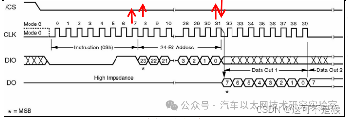
The “read data” command allows reading one byte or more bytes. First, pull the /CS pin low, then send 03h through the DIO pin to the chip, followed by sending the 24-bit address, which will be sampled by the chip on the rising edge of CLK. After the chip receives the 24-bit address, it will send the corresponding data from that address on the falling edge of the CLK pin from the DO pin, with the most significant bit first. After reading the data from this address, the address automatically increments, and the next address’s data will be sent out through the DO pin, forming a data stream. This means that as long as the clock is working, a single read command can read all the data from the chip’s storage area. Pull the /CS pin high to end the “read data” command. When the chip is executing programming, erasing, and reading status register commands, the “read data” command does not take effect.
Read Data Timing
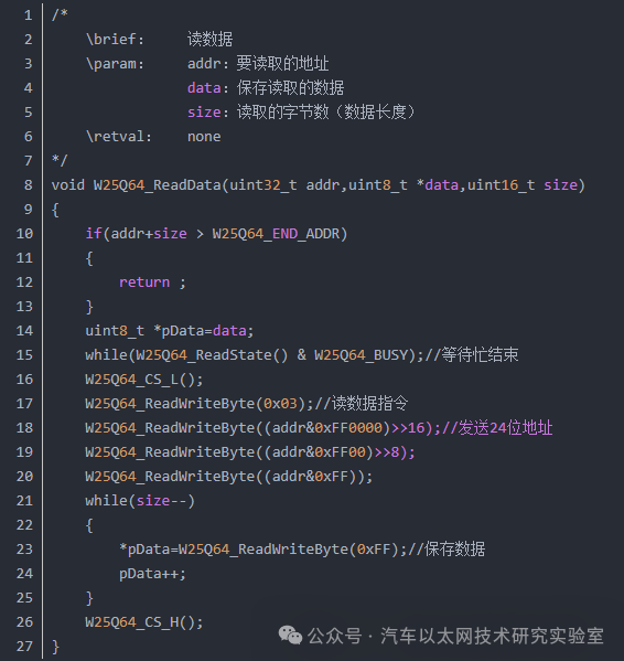
(1) Check if the address exceeds the maximum address range of FLASH.
(2) Wait for the busy signal to end.
(3) Pull the chip select low.
(4) Send the read data command 03H and the starting address of the data to be read.
(5) Continuously read data. Here, the size of data is set to one sector, allowing only one sector of data to be read.
(6) Pull the chip select high.
4.5 Page Programming (02H)
Before executing the “page programming” command, the “write enable” command must be executed, and the area to be written must be all 1s, meaning the area must be erased first. Pull the /CS pin low, then send the code 2h through the DIO pin to the chip, followed by sending the 24-bit address to the chip, and then send the bytes to be written to the chip. After writing the data, pull the /CS pin high.
After writing a page (256 bytes), the address must be reset to 0; otherwise, if the clock continues, the address will automatically become the starting address of the page. In some cases, if the number of bytes to be written is less than 256 bytes, the other written bytes will be meaningless. If the number of bytes to be written exceeds 256 bytes, the excess bytes will overwrite the previously written 256 bytes. Therefore, it is necessary to ensure that the number of bytes to be written is less than or equal to 256 bytes.
During the execution of the command, the “read status register” can be used to find that the BUSY bit is 1. When the command execution is complete, the BUSY bit automatically resets to 0. If the address to be written is in the “write protect” state, the “page programming” command will be invalid.
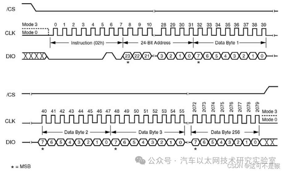
Page Programming Timing
During programming, a maximum of one page of data can be written at a time. After sending the programming command, the address to be written is sent directly, and the data to be written is sent immediately, with the address automatically offset. When writing the page programming function, it is assumed that the data to be written does not exceed one page, preventing data overwriting.
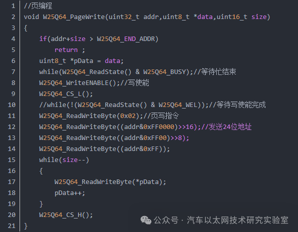
(1) Check if the address to be written exceeds the FLASH address range.
(2) Wait for the busy signal to end; this function does not “erase”, but the specific calling function may have called the “erase function” before, so it is necessary to wait for the erase to complete. Otherwise, the following commands will be invalid.
(3) Write enable. Execute the write enable command before performing page programming.
(4) Pull the chip select low.
(5) Send the page programming command, followed by sending the 24-bit FLASH address.
(6) Write the bytes to be written sequentially.
(7) Pull the chip select high. Page programming is complete.
4.5.1 Cross-Page Write Function (Ignoring Erase)
When writing data to W25Q64, only page write operations are supported. If more data needs to be written, it can only be written page by page to FLASH, which is inconvenient. W25Q64 does not have cross-page write functionality, but it can be written page by page. Based on this idea, a cross-page write function can be encapsulated.
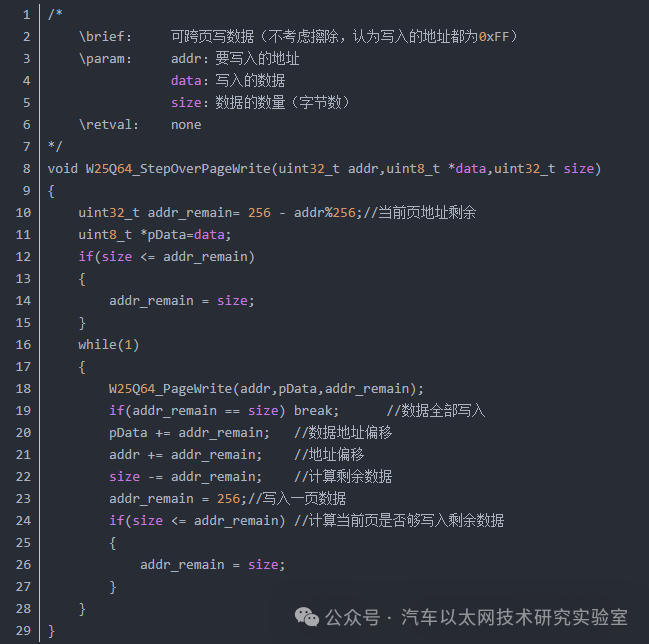
(1) Define a variable to record the current page’s remaining address, calculating the remaining address in the current page. For example: 0x00000F is the starting address of the data to be written. 0x000000~0x0000FF is the first page (256 bytes), with the address starting from 0x00000F to 0x0000FF, leaving 241 bytes of address space. 256-15%256=241.
(2) Check if the data to be written exceeds the remaining space in the current page. If it does not exceed, it means the current page is sufficient to write the amount of data to be written, and set addr_remain equal to the amount of data to be written. The addr_remain variable is significant in the current function; if the data to be written equals addr_remain, it means all data has been written.
(3) Write addr_remain bytes of data in the current page. addr_remain is a maximum of 256 bytes, which will not cause data overwriting, so no judgment is added in the page programming function.
(4) If addr_remain equals the data to be written, it indicates that the data has been completely written. Since the judgment was made in step (2), it will only be equal if the data to be written is less than the remaining amount in the current page.
(5) If the data has not been completely written, addr_remain bytes of data have been written, the data pointer is offset by addr_remain, and the FLASH address is offset by addr_remain (to the starting address of the next page), and the amount of data to be written is reduced by addr_remain.
(6) Calculate the remaining space in the current page (which is a full page of 256 bytes). 0x00000F+241=0x000100 (0x100=256), 256%256=0, 256-0=256.
(7) Check if the current page is sufficient to write the remaining data. If the remaining amount of data exceeds one page, it can only write one page of data, addr_remain = 256. If the current page is sufficient, write the remaining data.
(8) Repeat until all data is written.
4.5.2 Cross-Page Write (Considering Erase and Original Data)
In cross-page writing, the address is not considered for whether data can be written. Next, consider the erase issue. The erase function used is sector erase (4096 bytes), and the process is similar to cross-page writing. Sector erase will set all storage bits in the current sector to one, clearing all original data, so data backup should be done before the erase function.

The second sector
As shown, the address of the second sector has 16 pages. When writing data, if the first two pages of the current sector contain useful data, and data needs to be written to the third page of the current sector, the entire page will be erased (including valid data) during the sector erase, so the data of that page needs to be saved and written back in the end. Of course, if no erase is needed, it can be written directly to the second page.
-
/*
-
rief: Cross-page write data (considering erase and original data)
-
rief: addr: address to write to
-
data: data to write
-
size: number of data (in bytes)
-
etval: none -
*/
-
uint8_t sector_data[W25Q64_SECTOR_SIZE];
-
void W25Q64_WriteData(uint32_t addr,uint8_t *data,uint32_t size)
-
{
-
uint16_t sector_offset = addr%4096; // Calculate the address offset in the current sector
-
uint16_t sector_remain = 4096 – sector_offset; // Calculate the remaining space in the current sector
-
uint32_t sector_addr = addr – sector_offset; // Calculate the starting address of the current sector
-
uint8_t *pData=data;
-
uint32_t i;
-
if(size <= sector_remain)
-
{
-
sector_remain=(uint16_t )size;
-
}
-
while(1)
-
{
-
W25Q64_ReadData(addr,sector_data,sector_remain);// Read the data to be written from the address
-
for(i=0;i<sector_remain;i++)</sector_remain;i++)
-
{
-
if(sector_data[i]!=0xFF) break;
-
}
-
if(i!=sector_remain)// Check if the sector needs to be erased
-
{
-
// Save the current sector’s previous data before erasing
-
W25Q64_ReadData(sector_addr,sector_data,sector_offset);
-
// Save the current sector’s subsequent data before erasing
-
W25Q64_ReadData(addr + sector_remain,sector_data+(sector_offset+sector_remain),W25Q64_SECTOR_SIZE – (sector_offset+sector_remain));
-
W25Q64_SectorErase(sector_addr);// Erase the sector
-
// Insert the data to be written into the buffer
-
for(i=0;i<sector_remain;i++)</sector_remain;i++)
-
{
-
sector_data[sector_offset+i]= pData[i];
-
}
-
W25Q64_StepOverPageWrite(sector_addr,sector_data,W25Q64_SECTOR_SIZE);
-
sector_offset = 0;
-
}
-
else
-
{
-
W25Q64_StepOverPageWrite(addr,pData,sector_remain);// Write data to the current sector
-
}
-
if(sector_remain == size) break;// All data has been completely written
-
pData += sector_remain; // Offset the data address
-
addr += sector_remain; // Offset the flash address
-
sector_addr = addr; // Current sector starting address
-
size -= sector_remain; // Reduce the amount of data
-
sector_remain = W25Q64_SECTOR_SIZE;// Remaining space in the current sector
-
if(size <= W25Q64_SECTOR_SIZE)// Check if the current sector is sufficient to write the remaining data
-
{
-
sector_remain = size;
-
}
-
}
-
}
Example: Write 4096 bytes of data starting from address 0x001300.

(1) Calculate the offset of the starting address to be written in the current page (768), the remaining space in the sector (3328), and the starting address of the current sector (0x001000).
(2) Check if the current sector is sufficient to write 4096 bytes of data. Clearly, it is not sufficient.
(3) Read the data from 0x001300~0x001FFF (3328 bytes) and check for any non-0xFF values.
(4) No need to erase, directly write 3328 bytes of data sequentially to address 0x001300.
(5) Erase is needed; read the first half of the address (0x001000~0x000FFF) data and keep it in the buffer, and the second half of the data (since it needs to fill the sector, there is no data to save in the second half). Then save the 3328 bytes of data to the first half of the buffer.
(6) Data has not been completely written, with 768 bytes remaining (4096-3328).
(7) Offset the data address and flash address, changing the current sector address (to 0x002000), reducing the amount of data to be written by 3328 bytes, and the current page has 4096 bytes of space remaining.
(8) The current page is sufficient to write the remaining data, setting addr_remain=size. Then return to (2).
Calling this function allows for direct cross-page writing of data in FLASH with built-in erase functionality, ensuring that data is not lost due to sector erasure during multiple write operations.
5. Practical Testing
Here, data is written to both sides of address 0x200000, as 0x200000 is the starting address of the next sector (other two sectors can also be chosen). Write 5 bytes of data continuously at address 0x200000-10, and then cross-sector write 25 bytes of data from address 0x200000-5, totaling 30 bytes of data written.
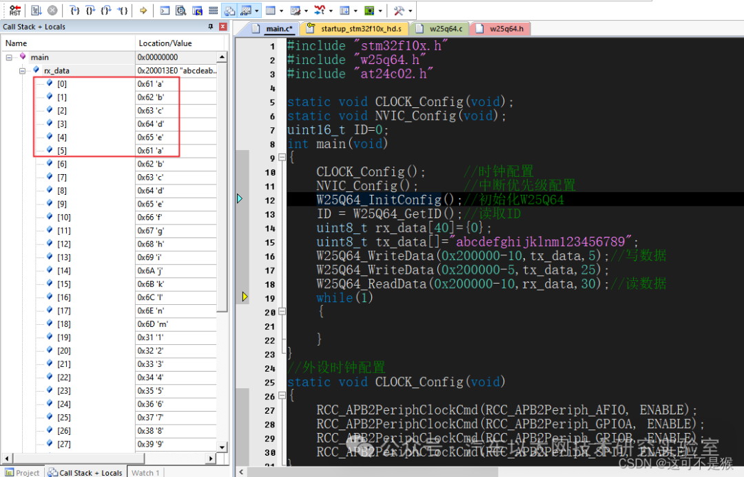
It can be seen that the first five bytes of data read “abcde” are the same as the data written the first time, and they have not been cleared by the second write operation. The second write operation can also achieve cross-page data writing.
Application:
Using W25Q64 to store font libraries and call them in the LCD.




*Disclaimer: This article is original or forwarded by the author.If it inadvertently infringes on someone’s intellectual property, please inform us and we will delete it.The above images and text are sourced from the internet; if there is any infringement, please contact us in a timely manner, and we will delete it within 24 hours.The content of the article represents the author’s personal views, and the Automotive Ethernet Technology Research Laboratory reprints it only to convey a different perspective, not representing the Automotive Ethernet Technology Research Laboratory’s endorsement or support of this view. If there are any objections, please contact the Automotive Ethernet Technology Research Laboratory.
Original link:
https://blog.csdn.net/we_long/article/details/131782390