In Xilinx FPGA design, Block Random Access Memory (Block RAM, BRAM) is a core hard storage resource. The Block Memory Generator IP core provided by Vivado 2021 encapsulates the underlying hard logic of BRAM, allowing for quick configuration into single/dual-port RAM/ROM types without the need to manually write storage array logic, combining convenience and stability. This article is based on the XC7Z015CLG485-2I hardware platform, focusing on the Block Memory Generator IP core, detailing the configuration, instantiation, and engineering applications of BRAM.
01
—
BRAM Implementation Principles (Based on IP Core)
The core granularity of BRAM in Xilinx FPGA is 36Kb (which can be split into 2 x 18Kb). The Block Memory Generator IP core essentially provides a visual configuration encapsulation of the BRAM hard core: through the IP core, BRAM types (RAM/ROM), port structures (single/dual-port), bit width x depth, initialization files, clock/reset modes, and other parameters can be quickly defined. The IP core automatically generates instantiation templates compatible with Verilog 95 standards, while the underlying implementation still relies on BRAM’s storage array, address decoding, and read/write control logic for data access. Compared to manually writing storage arrays, the IP core can avoid issues such as timing non-convergence and resource wastage, making it the preferred method for engineering development.
02
—
Types and Configuration of BRAM Cores
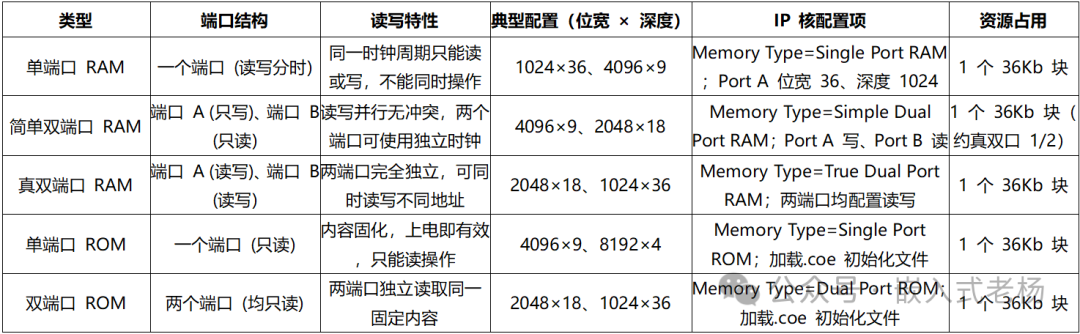
The Block Memory Generator IP core supports configurations for single-port RAM/ROM, simple dual-port RAM, true dual-port RAM/ROM, etc. The core features and key parameter correspondence of the IP core configuration are shown in the table below:
03
—
BRAM Application Cases (IP Core Implementation)
1. Single-Port RAM Application Case
Function Introduction:
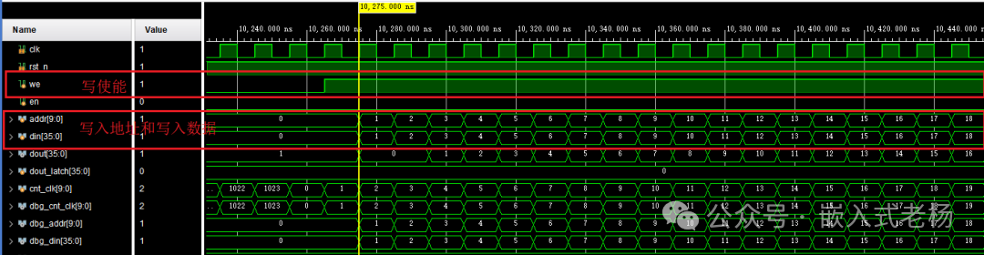
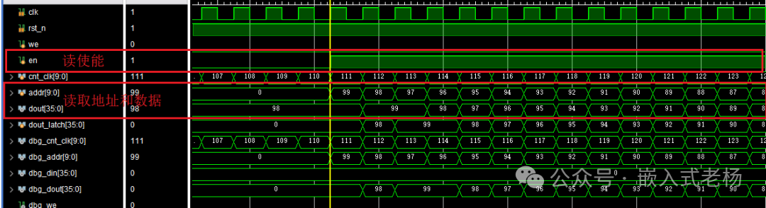
Based on the Xilinx FPGA, the Block Memory Generator IP core implements precise read/write testing of a single-port 36Kb BRAM. In the write phase (counter 0~99 cycles), data 0~99 is sequentially written to RAM addresses 0~99, with addresses and data strictly corresponding one-to-one; in the read phase (counter 110~209 cycles), data is read back from addresses 99~0 in reverse order.
IP Core Configuration Steps:
-
Open Vivado 2021, search for “Block Memory Generator” in the IP Catalog and add it;
-
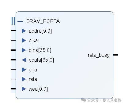
Configure the Basic page: Memory Type=Single Port RAM, Interface Type=Simple;
-
Configure Port A Options: Write Width=36, Write Depth=1024, Read Width=36, Read Depth=1024;
-
Configure Other Options: Enable Reset, Reset Type=Synchronous, Reset Polarity=Low;
-
Click “Generate Output Products” to generate the IP core files, selecting Verilog language.
IP Core Instantiation Code (single_port_ram_ip.v):
module single_port_ram_ip( input clk, // 100MHz clock input rst_n, // Active low reset input we, // Write enable (active high) input en, // Read enable (active high) input [9:0] addr, // 10-bit address bus input [35:0] din, // 36-bit write data output [35:0] dout // 36-bit read data (synchronous read, 1 cycle delay);wire rsta_busy; // Reset busy signal (provided by IP core, no need to use) // Instantiate Block Memory Generator IP core (single-port RAM)blk_mem_gen_0 your_instance_name ( .clka(clk), // Clock input .rsta(~rst_n), // Reset (IP core active high, inverted to adapt to external active low) .ena(en | we), // Enable (valid during read/write) .wea(we), // Write enable .addra(addr), // Address input .dina(din), // Write data .douta(dout), // Read data (synchronous read, 1 cycle delay) .rsta_busy(rsta_busy) // Reset busy signal (not used));endmoduleTop-Level Call File (top_single_port_ram.v):
module top_single_port_ram( input clk, // 100MHz clock input input rst_n // Active low reset input); // Internal signal definitionsreg we; // Write enable (active high)reg en; // Read enable (active high)reg [9:0] addr; // 10-bit address register (0~1023)reg [35:0] din; // 36-bit write datawire [35:0] dout; // BRAM raw output (synchronous read, address updated after 1 cycle)reg [35:0] dout_latch; // Read data latch (matches BRAM 1 cycle delay, precisely corresponding to address)reg [9:0] cnt_clk; // Clock counter (controls read/write phase) /** * Clock counter: reset to zero, increments every cycle after reset release * 1 count = 10ns (100MHz clock cycle), precisely divides read/write phase */always @(posedge clk or negedge rst_n) begin if(!rst_n) begin cnt_clk <= 10'd0; end else begin cnt_clk <= cnt_clk + 1'b1; endend /** * Core read/write control logic (three phases): * 1. Write phase (cnt_clk=0~99): addr=0~99, din=0~99 * 2. Read phase (cnt_clk=110~209): addr=99~0, dout_latch=99~0 (matches 1 cycle delay) * 3. Final phase (cnt_clk≥210): disable enable, reset signal */always @(posedge clk or negedge rst_n) begin if(!rst_n) begin // Reset initialization we <= 1'b0; en <= 1'b0; addr <= 10'd0; din <= 36'd0; dout_latch <= 36'd0; end else begin // -------------------------- Write phase: cnt_clk=0~99 -------------------------- if(cnt_clk < 100) begin we <= 1'b1; // Write enable valid en <= 1'b0; // Read enable disabled addr <= cnt_clk; // Address = counter (0~99) din <= {18'd0, cnt_clk}; // Data = 0~99 (high 18 bits padded with 0) dout_latch <= 36'd0; // Read latch cleared end // -------------------------- Read phase: cnt_clk=110~209 -------------------------- else if(cnt_clk >= 110 && cnt_clk < 210) begin we <= 1'b0; // Write enable disabled en <= 1'b1; // Read enable valid // Read address control: set to 99 at 110 cycles, decrement by 1 each cycle (99→0) if(cnt_clk == 110) begin addr <= 10'd99; // Starting address = 99 (last valid address in write phase) end else begin addr <= addr - 1'b1; // Address decremented by 1 end // Data latch: matches BRAM 1 cycle synchronous read delay // - cnt_clk=110: addr=99 → dout valid at 111 cycles → latch 99 at 111 cycles // - cnt_clk=111: addr=98 → dout valid at 112 cycles → latch 98 at 112 cycles // - ... and so on, final dout_latch=99~0 if(cnt_clk > 110) begin // Skip the first cycle (wait for dout to be valid) dout_latch <= dout; end end // -------------------------- Final phase: cnt_clk≥210 -------------------------- else begin we <= 1'b0; en <= 1'b0; addr <= 10'd0; din <= 36'd0; dout_latch <= 36'd0; end endend // Instantiate IP core encapsulation modulesingle_port_ram_ip u_single_port_ram_ip( .clk (clk), .rst_n (rst_n), .we (we), .en (en), .addr (addr), .din (din), .dout (dout)); // Debug signals (for ILA or simulation observation)wire [9:0] dbg_cnt_clk = cnt_clk;wire [9:0] dbg_addr = addr;wire [35:0] dbg_din = din;wire [35:0] dbg_dout = dout_latch;wire dbg_we = we;wire dbg_en = en;endmodule
Timing Constraint File (constraints.xdc):
# Clock constraint: 100MHz (period 10ns)create_clock -name clk -period 10.000 -waveform {0.000 5.000} [get_ports clk] # Pin constraintsset_property PACKAGE_PIN L5 [get_ports clk] // Clock pin L5set_property PACKAGE_PIN H5 [get_ports rst_n] // Reset pin H5 # IO standard: 3.3V LVCMOSset_property IOSTANDARD LVCMOS33 [get_ports {clk rst_n}] # Auxiliary constraints: reduce power consumptionset_property PULLUP false [get_ports *]set_property CONFIG.VOLTAGE 3.3 [current_design]
Simulation Test File (tb_single_port_ram.v):
`timescale 1ns/1ps module tb_single_port_ram;reg clk; // 100MHz simulation clockreg rst_n; // Active low simulation resetwire [35:0] dout_latch; // Observed read data (should be 99~0)wire [9:0] dbg_cnt_clk; // Counterwire [9:0] dbg_addr; // Address // Generate 100MHz clock (period 10ns)initial begin clk = 1'b0; forever #5 clk = ~clk;end // Reset control: 0~20ns reset valid, release after 20nsinitial begin rst_n = 1'b0; #20 rst_n = 1'b1; #2100 $stop; // Simulate to 2120ns (covering read phase 110~209)end // Instantiate top-level moduletop_single_port_ram u_top_single_port_ram( .clk (clk), .rst_n (rst_n)); // Export observed signalsassign dbg_cnt_clk = u_top_single_port_ram.cnt_clk;assign dbg_addr = u_top_single_port_ram.addr;assign dout_latch = u_top_single_port_ram.dout_latch;endmoduleRun Results:
In the RTL simulation, the reset signal is valid from 0 to 20ns, and after release, the counter starts incrementing from 0; during the write phase, the counter from 0 to 99 corresponds to RAM addresses 0 to 99 and write data 0 to 99; in the read phase, at counter 110, the address is initialized to 99, and subsequently, the address decrements by 1, starting from cycle 111, latching the BRAM output data, precisely matching the 1 cycle delay of synchronous read, ultimately reading the data corresponding to addresses 99 to 0 sequentially as 99 to 0.
2. Simple Dual-Port RAM Application Case
Function Introduction:
Based on the IP core, a simple dual-port RAM of 4096×9 bits is implemented, where Port A is the write port and Port B is the read port. Under a 100MHz clock, parallel read and write operations occur without conflict. When write enable is valid, 9-bit data is written to Port A, and when read enable is valid, data is synchronously read from Port B.
IP Core Configuration Steps:
-
Open the Block Memory Generator IP core, configure the Basic page: Memory Type=Simple Dual Port RAM;
-
Port A Options: Write Width=9, Write Depth=4096;
-
Port B Options: Read Width=9, Read Depth=4096;
-
Enable synchronous reset (active low), generate Verilog 95 compatible IP core files.
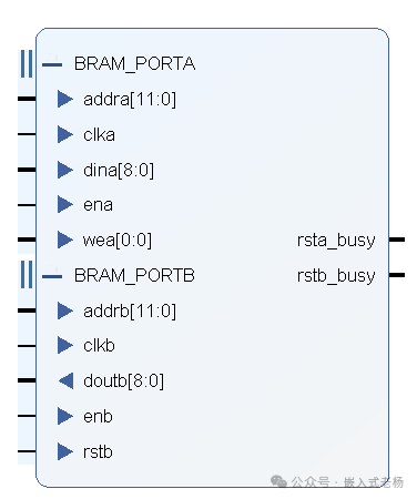
IP Core Instantiation Code (simple_dual_port_ram_ip.v):
module simple_dual_port_ram_ip( input clk_a, // Write port clock input we_a, // Write enable input [11:0] addr_a, // Write address input [8:0] din_a, // Write data input clk_b, // Read port clock input rst_n_b, // Read port reset input en_b, // Read enable input [11:0] addr_b, // Read address output [8:0] dout_b // Read data); // IP core reset busy signals (only as internal signals, not exported)wire rsta_busy,rstb_busy; // Instantiate Simple Dual Port RAM IP coreblk_mem_gen_0 u_blk_mem_gen_0( .clka (clk_a), .ena (we_a), .wea (we_a), .addra (addr_a), .dina (din_a), .clkb (clk_b), .rstb (~rst_n_b), .enb (en_b), .addrb (addr_b), .doutb (dout_b), .rsta_busy (rsta_busy), // Internal signal, not exported .rstb_busy (rstb_busy) // Internal signal, not exported);endmoduleTop-Level Call File (top_simple_dual_port_ram.v):
module top_simple_dual_port_ram( input clk, // Hardware pin L5 input rst_n // Hardware pin H5); // Internal signal definitionsreg we_a; // Port A write enablereg [11:0] addr_a; // Port A write addressreg [8:0] din_a; // Port A write datareg en_b; // Port B read enablereg [11:0] addr_b; // Port B read addresswire [8:0] dout_b; // Port B read data // Instantiate IP core encapsulation module (remove unnecessary rsta_busy/rstb_busy port connections)simple_dual_port_ram_ip u_simple_dual_port_ram_ip( .clk_a (clk), // Write clock = system clock .we_a (we_a), // Write enable connection .addr_a (addr_a), // Write address connection .din_a (din_a), // Write data connection .clk_b (clk), // Read clock = system clock (synchronous) .rst_n_b (rst_n), // Read reset = global reset .en_b (en_b), // Read enable connection .addr_b (addr_b), // Read address connection .dout_b (dout_b) // Read data connection); // Test logic: Port A writes data, Port B synchronously follows the read addressalways @(posedge clk or negedge rst_n) begin if(!rst_n) begin we_a <= 1'b0; // Reset disables write enable en_b <= 1'b0; // Reset disables read enable addr_a <= 12'd0; // Write address initialization addr_b <= 12'd0; // Read address initialization din_a <= 9'd0; // Write data initialization end else begin we_a <= 1'b1; // Continuously enable write enable en_b <= 1'b1; // Continuously enable read enable addr_a <= addr_a + 1'b1; // Write address increments each cycle addr_b <= addr_a; // Read address follows current write address din_a <= addr_a[8:0]; // Write data = low 9 bits of write address endendendmodule
Timing Constraints:
# Constraint clk pin as 100MHz system clock, period 10ns (50% duty cycle)create_clock -name clk -period 10.000 -waveform {0.000 5.000} [get_ports clk] # -------------------------- Pin location constraints --------------------------set_property PACKAGE_PIN L5 [get_ports clk] // Clock pin L5set_property PACKAGE_PIN H5 [get_ports rst_n] // Reset pin H5 # -------------------------- IO level standard constraints --------------------------set_property IOSTANDARD LVCMOS33 [get_ports {clk rst_n}] # -------------------------- Auxiliary constraints --------------------------set_property PULLUP false [get_ports *] // Disable pull-up on unused pinsset_property CONFIG.VOLTAGE 3.3 [current_design] // Configure core voltage 3.3VSimulation File:
`timescale 1ns/1ps module tb_simple_dual_port_ram; // Simulation signal definitionsreg clk; // 100MHz simulation clockreg rst_n; // Active low simulation resetwire [8:0] dout_b; // Port B read datawire [11:0] dbg_addr_a; // Write address debug signalwire [8:0] dbg_din_a; // Write data debug signalwire [11:0] dbg_addr_b; // Read address debug signalwire dbg_we_a; // Write enable debug signalwire dbg_en_b; // Read enable debug signal /** * 100MHz clock generation: period 10ns (5ns high, 5ns low) */initial begin clk = 1'b0; forever #5 clk = ~clk;end /** * Reset control: 0~20ns reset valid, 20ns after release */initial begin rst_n = 1'b0; #20 rst_n = 1'b1; #2000 $stop; // 2020ns stop simulationend // Instantiate top-level moduletop_simple_dual_port_ram u_top_simple_dual_port_ram( .clk (clk), .rst_n (rst_n)); // Export debug signals (for simulation observation)assign dbg_addr_a = u_top_simple_dual_port_ram.addr_a;assign dbg_din_a = u_top_simple_dual_port_ram.din_a;assign dbg_addr_b = u_top_simple_dual_port_ram.addr_b;assign dbg_we_a = u_top_simple_dual_port_ram.we_a;assign dbg_en_b = u_top_simple_dual_port_ram.en_b;endmoduleRTL Simulation Results:
In the simulation, Port A writes 9-bit data to addresses 0~199, and Port B reads the corresponding data with a 1 clock cycle delay, with no read/write conflicts; during board-level verification, timing converges, and resource usage is 1 x 36Kb BRAM block.
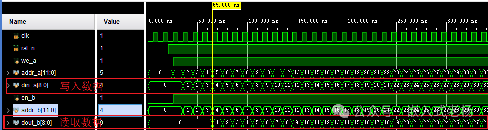
The Xilinx Simple Dual Port RAM IP core has an inherent synchronous read delay (the read address must wait 1 clock cycle after being updated to output the corresponding data), combined with the timing logic in the code where the write address increments each cycle and the read address synchronously follows the write address, resulting in multiple cycles needed to output valid data after the read address is updated..
3. True Dual-Port RAM Application Case
Function Introduction:
Based on the IP core, a true dual-port RAM of 2048×18 bits is implemented, where both ports support read and write operations. Under a 100MHz clock, different addresses can be read and written simultaneously. When reading and writing the same address, writing takes priority, and outputs are cleared on reset. After the reset is released, pure write operations are performed first, with both ports writing corresponding values to addresses 0~99 (address N writes data N). After filling, the write_done flag is used to switch to the pure read phase, disabling write enable and maintaining global enable, with both port addresses cycling through 0~99 to continuously read the written data.
IP Core Configuration Steps:
-
Block Memory Generator IP core Basic page: Memory Type=True Dual Port RAM;
-
Port A/B Options: Write/Read Width=18, Write/Read Depth=2048;
-
Enable two-port synchronous reset (active low), generate IP core files.
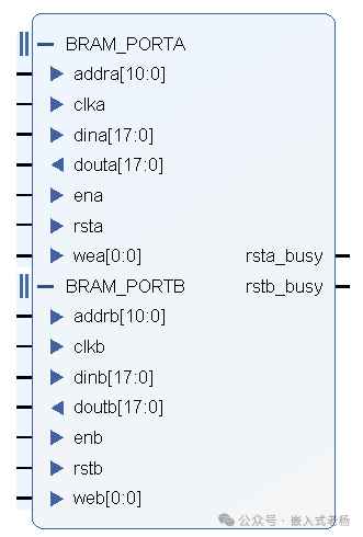
IP Core Instantiation Code (true_dual_port_ram_ip.v):
module true_dual_port_ram_ip( input clk_a, // Port A clock (100MHz) input rst_n_a, // Port A active low reset input we_a, // Port A write enable (active high) input en_a, // Port A global enable (active high, prerequisite for read/write operations) input [10:0] addr_a, // Port A address (11 bits, addressing range 0~2047) input [17:0] din_a, // Port A write data (18 bits) output [17:0] dout_a, // Port A read data (18 bits, synchronous read delay 1 cycle) input clk_b, // Port B clock (100MHz, synchronous with A) input rst_n_b, // Port B active low reset input we_b, // Port B write enable (active high) input en_b, // Port B global enable (active high, prerequisite for read/write operations) input [10:0] addr_b, // Port B address (11 bits, addressing range 0~2047) input [17:0] din_b, // Port B write data (18 bits) output [17:0] dout_b // Port B read data (18 bits, synchronous read delay 1 cycle); // Internal reset busy signals (only for internal connections, no need to export)wire rsta_busy;wire rstb_busy; // Instantiate Xilinx True Dual Port RAM IP coreblk_mem_gen_0 u_blk_mem_gen_0( .clka (clk_a), .rsta (~rst_n_a), // IP core reset active high, inverted to adapt to external active low reset .ena (en_a), // Port A global enable .wea (we_a), // Port A write enable .addra (addr_a), // Port A address .dina (din_a), // Port A write data .douta (dout_a), // Port A raw read data (not compensating for synchronous delay) .clkb (clk_b), // Port B clock .rstb (~rst_n_b), // IP core reset active high, inverted to adapt to external active low reset .enb (en_b), // Port B global enable .web (we_b), // Port B write enable .addrb (addr_b), // Port B address .dinb (din_b), // Port B write data .doutb (dout_b), // Port B raw read data (not compensating for synchronous delay) .rsta_busy (rsta_busy), // Reset busy signal (internal) .rstb_busy (rstb_busy) // Reset busy signal (internal);endmoduleTop-Level Call File (top_true_dual_port_ram.v):
module top_true_dual_port_ram( input clk, // 100MHz clock input input rst_n // Active low reset input); // -------------------------- Internal signal definitions -------------------------- // Port A core signalsreg we_a; // Port A write enable (active high)reg en_a; // Port A global enable (active high)reg [10:0] addr_a; // Port A address (11 bits)reg [17:0] din_a; // Port A write data (18 bits)wire [17:0] dout_a; // Port A raw read data (synchronous read delay 1 cycle)reg [17:0] dout_a_latch; // Port A read data latch (compensates for synchronous read delay)reg write_done_a; // Port A write phase completion flag (1=write complete, enter read phase) // Port B core signalsreg we_b; // Port B write enable (active high)reg en_b; // Port B global enable (active high)reg [10:0] addr_b; // Port B address (11 bits)reg [17:0] din_b; // Port B write data (18 bits)wire [17:0] dout_b; // Port B raw read data (synchronous read delay 1 cycle)reg [17:0] dout_b_latch; // Port B read data latch (compensates for synchronous read delay)reg write_done_b; // Port B write phase completion flag (1=write complete, enter read phase) // -------------------------- IP core instantiation --------------------------true_dual_port_ram_ip u_true_dual_port_ram_ip( .clk_a (clk), // Read/write clock unified to 100MHz system clock .rst_n_a (rst_n), // Port A reset reused global reset .we_a (we_a), // Port A write enable connection .en_a (en_a), // Port A global enable connection .addr_a (addr_a), // Port A address connection .din_a (din_a), // Port A write data connection .dout_a (dout_a), // Port A raw read data connection .clk_b (clk), // Port B clock synchronized with Port A .rst_n_b (rst_n), // Port B reset reused global reset .we_b (we_b), // Port B write enable connection .en_b (en_b), // Port B global enable connection .addr_b (addr_b), // Port B address connection .din_b (din_b), // Port B write data connection .dout_b (dout_b) // Port B raw read data connection); // -------------------------- Port A write then read control logic --------------------------always @(posedge clk or negedge rst_n) begin if(!rst_n) begin // Reset initialization: all signals cleared, write phase not completed we_a <= 1'b0; en_a <= 1'b0; addr_a <= 11'd0; din_a <= 18'd0; write_done_a <= 1'b0; dout_a_latch <= 18'd0; end else begin // Phase 1: pure write phase (addr_a 0~99, not written yet) if(!write_done_a) begin en_a <= 1'b1; // Global enable set to 1 (prerequisite for write operation) we_a <= 1'b1; // Write enable set to 1 (only for write operation) din_a <= 18'd0 + addr_a; // Write data = address value (0~99, compatible with Verilog-2001) // Address increments until filled 0~99 if(addr_a < 11'd99) begin addr_a <= addr_a + 1'b1; write_done_a <= 1'b0; // Not written yet, mark remains 0 end else begin addr_a <= 11'd99; // Address stops at 99 (last write address) write_done_a <= 1'b1; // Filled 0~99, mark write complete end end // Phase 2: pure read phase (only read operation after write is complete) else begin en_a <= 1'b1; // Global enable remains 1 (prerequisite for read operation) we_a <= 1'b0; // Write enable set to 0 (close write, only read) din_a <= 18'd0; // Write closed, data meaningless // Read address cycles 0~99, continuously read written data if(addr_a == 11'd99) begin addr_a <= 11'd0; // Address resets to 0 after reaching 99 end else begin addr_a <= addr_a + 1'b1; // Address increments end dout_a_latch <= dout_a; // Latch raw read data, compensating for synchronous read 1 cycle delay end endend // -------------------------- Port B write then read control logic (identical to A) --------------------------always @(posedge clk or negedge rst_n) begin if(!rst_n) begin // Reset initialization: all signals cleared, write phase not completed we_b <= 1'b0; en_b <= 1'b0; addr_b <= 11'd0; din_b <= 18'd0; write_done_b <= 1'b0; dout_b_latch <= 18'd0; end else begin // Phase 1: pure write phase (addr_b 0~99, not written yet) if(!write_done_b) begin en_b <= 1'b1; // Global enable set to 1 (prerequisite for write operation) we_b <= 1'b1; // Write enable set to 1 (only for write operation) din_b <= 18'd0 + addr_b; // Write data = address value (0~99, compatible with Verilog-2001) // Address increments until filled 0~99 if(addr_b < 11'd99) begin addr_b <= addr_b + 1'b1; write_done_b <= 1'b0; // Not written yet, mark remains 0 end else begin addr_b <= 11'd99; // Address stops at 99 (last write address) write_done_b <= 1'b1; // Filled 0~99, mark write complete end end // Phase 2: pure read phase (only read operation after write is complete) else begin en_b <= 1'b1; // Global enable remains 1 (prerequisite for read operation) we_b <= 1'b0; // Write enable set to 0 (close write, only read) din_b <= 18'd0; // Write closed, data meaningless // Read address cycles 0~99, continuously read written data if(addr_b == 11'd99) begin addr_b <= 11'd0; // Address resets to 0 after reaching 99 end else begin addr_b <= addr_b + 1'b1; // Address increments end dout_b_latch <= dout_b; // Latch raw read data, compensating for synchronous read 1 cycle delay end endend // -------------------------- Debug signal export (for simulation observation) --------------------------wire [17:0] dbg_dout_a = dout_a_latch; // Port A final read data (compensated for synchronous delay)wire [17:0] dbg_dout_b = dout_b_latch; // Port B final read data (compensated for synchronous delay)wire [10:0] dbg_addr_a = addr_a; // Port A current addresswire [10:0] dbg_addr_b = addr_b; // Port B current addresswire dbg_write_done_a = write_done_a; // Port A write completion flagwire dbg_write_done_b = write_done_b; // Port B write completion flagendmodule
Timing Constraints:
create_clock -name clk -period 10.000 -waveform {0.000 5.000} [get_ports clk] # -------------------------- Pin location constraints --------------------------# Clock pin: hardware pin L5 (consistent with code comments, adapted to FPGA board layout)set_property PACKAGE_PIN L5 [get_ports clk]# Reset pin: hardware pin H5 (active low, consistent with code comments)set_property PACKAGE_PIN H5 [get_ports rst_n] # -------------------------- IO level standard constraints --------------------------# clk/rst_n use LVCMOS33 level standard (3.3V), adapted to FPGA general IO voltage specificationsset_property IOSTANDARD LVCMOS33 [get_ports {clk rst_n}] # -------------------------- Auxiliary constraints --------------------------# Disable pull-up resistors on unused pins, reduce FPGA static power consumptionset_property PULLUP false [get_ports *]# Configure FPGA core voltage to 3.3V, matching IO level standard to avoid level mismatch issuesset_property CONFIG.VOLTAGE 3.3 [current_design]# Mark reset signal as active low, assisting synthesis tools to optimize reset logic (reduce glitches)set_property CONFIG.POLARITY LOW [get_ports rst_n]RTL Simulation File:
`timescale 1ns/1ps module tb_true_dual_port_ram; // Simulation signal definitionsreg clk; // 100MHz simulation clock (shared by Port A/B)reg rst_n; // Active low simulation reset (shared by Port A/B) // Core observation signals (read data compensated for synchronous delay)wire [17:0] dbg_dout_a; // Port A final read datawire [17:0] dbg_dout_b; // Port B final read data // Auxiliary debug signalswire [10:0] dbg_addr_a; // Port A current addresswire [10:0] dbg_addr_b; // Port B current addresswire dbg_write_done_a; // Port A write completion flagwire dbg_write_done_b; // Port B write completion flagwire dbg_we_a; // Port A write enablewire dbg_we_b; // Port B write enable /** * 100MHz clock generation: period 10ns (5ns high, 5ns low) * Forever loop flip, fully matches FPGA hardware clock frequency */initial begin clk = 1'b0; // Initial clock low forever #5 clk = ~clk; // Flip every 5ns, generating 100MHz clockend /** * Reset signal control: * - 0~20ns: reset valid (low), initialize all registers * - 20ns after: reset release, start "write then read" logic * - 4000ns: end simulation (covering write 0~99 + multiple rounds of read 0~99) */initial begin rst_n = 1'b0; // Initial reset valid #20 rst_n = 1'b1; // Release reset after 20ns #4000 $stop; // Stop simulation at 4020ns, ensuring complete observation of read/write cycleend // Instantiate top-level moduletop_true_dual_port_ram u_top_true_dual_port_ram( .clk (clk), .rst_n (rst_n)); // Export debug signals (for simulation waveform observation)assign dbg_dout_a = u_top_true_dual_port_ram.dbg_dout_a;assign dbg_dout_b = u_top_true_dual_port_ram.dbg_dout_b;assign dbg_addr_a = u_top_true_dual_port_ram.dbg_addr_a;assign dbg_addr_b = u_top_true_dual_port_ram.dbg_addr_b;assign dbg_write_done_a = u_top_true_dual_port_ram.dbg_write_done_a;assign dbg_write_done_b = u_top_true_dual_port_ram.dbg_write_done_b;assign dbg_we_a = u_top_true_dual_port_ram.we_a;assign dbg_we_b = u_top_true_dual_port_ram.we_b;endmoduleRun Results:
In the RTL simulation, the reset signal remains low valid from 0 to 20ns, initializing all registers to zero; after the reset is released at 20ns, the pure write phase begins, with Port A/Port B’s write enables (we_a/we_b) and global enables (en_a/en_b) set to 1, addresses incrementing from 0 to 99, writing data that synchronously matches the address values (0~99). When the address reaches 99, write_done_a/write_done_b is set to 1, marking the completion of the write phase; after the write phase ends, it switches to the pure read phase, with write enables closed and global enables remaining high, both ports cycling through addresses 0~99, with the latched read data (dbg_dout_a/dbg_dout_b) strictly corresponding to their addresses (address N corresponds to data N).
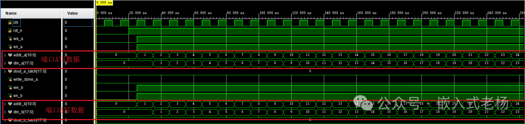
4. Single-Port ROM Application Case
Function Introduction:
Based on the IP core, a single-port ROM of 4096×12 bits is implemented, solidifying a table of 12-bit values from 0 to 4095 through a .coe file. Under a 100MHz clock, when read enable is valid, the solidified data is read out, and outputs are cleared on reset.
Preparation:
Write a .coe initialization file (rom_4096x12.coe):
memory_initialization_radix=10; // Decimalmemory_initialization_vector=0,1,2,3,...,4095; // Complete list from 0 to 4095, omitted intermediate valuesIP Core Configuration Steps:
-
Block Memory Generator IP core Basic page: Memory Type=Single Port ROM;
-
Port A Options: Read Width=12, Read Depth=4096;
-
Other Options: Load Init File, select the above rom_4096x9.coe file;
-
Enable synchronous reset (active low), generate IP core files.
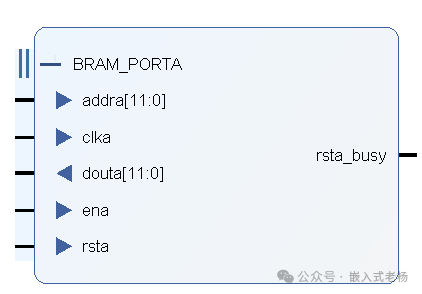
IP Core Instantiation Code (single_port_rom_ip.v):
module single_port_rom_ip( input clk, // 100MHz clock input rst_n, // Active low reset input en, // Read enable input [11:0] addr, // Address bus (12 bits, 0~4095) output [12:0] dout // Read data (12 bits)); // Correction: remove extra bracket at the endwire rsta_busy; // Instantiate single-port ROM IP core (blk_mem_gen_0 is the module name generated by the IP core)blk_mem_gen_0 u_blk_mem_gen_0( .clka (clk), // ROM synchronous read clock .rsta (~rst_n), // IP core reset active high, inverted to adapt to external active low reset .ena (en), // ROM read enable .addra (addr), // ROM read address .douta (dout), // ROM read data output .rsta_busy(rsta_busy) // output wire rsta_busy);endmoduleTop-Level Call File (top_single_port_rom.v):
module top_single_port_rom( input clk, // Pin L5: 100MHz clock input input rst_n // Pin H5: Active low reset input); // Correction: remove extra bracket at the end // Internal signal definitionsreg en; // ROM read enablereg [11:0] addr; // ROM read address (12 bits, 0~4095)wire [11:0] dout; // ROM read data (12 bits) // Instantiate ROM IP core encapsulation modulesingle_port_rom_ip u_single_port_rom_ip( .clk (clk), .rst_n (rst_n), .en (en), .addr (addr), .dout (dout)); // Test logic: cyclically read ROM addresses 0~4095always @(posedge clk or negedge rst_n) begin if(!rst_n) begin en <= 1'b0; // Disable read enable on reset addr <= 12'd0; // Reset address to zero end else begin en <= 1'b1; // Continuously enable read operation after reset release // Address cycles 0~4095: reset to 0 after reaching 4095, otherwise increment addr <= (addr == 12'd4095) ? 12'd0 : addr + 1'b1; endendendmoduleTiming Constraints:
create_clock -name clk -period 10.000 -waveform {0.000 5.000} [get_ports clk] # -------------------------- Pin location constraints --------------------------# Clock pin: hardware pin L5 (consistent with code comments)set_property PACKAGE_PIN L5 [get_ports clk]# Reset pin: hardware pin H5 (active low, consistent with code comments)set_property PACKAGE_PIN H5 [get_ports rst_n] # -------------------------- IO level standard constraints --------------------------# clk/rst_n use LVCMOS33 level standard (3.3V), adapted to FPGA general IO voltageset_property IOSTANDARD LVCMOS33 [get_ports {clk rst_n}] # -------------------------- Auxiliary constraints --------------------------# Disable pull-up resistors on unused pins, reduce FPGA power consumptionset_property PULLUP false [get_ports *]# Configure FPGA core voltage to 3.3V, matching IO level standardset_property CONFIG.VOLTAGE 3.3 [current_design] # -------------------------- ROM timing optimization constraints --------------------------# Constrain ROM read data output delay, ensure timing convergence under 100MHz clockset_max_delay 9.0 -from [get_ports addr] -to [get_ports dout]
RTL Simulation File:
`timescale 1ns/1ps module tb_single_port_rom; // Simulation signal definitionsreg clk; // 100MHz simulation clockreg rst_n; // Active low simulation resetwire [11:0] dout; // ROM read data (core observation)wire [11:0] dbg_addr; // ROM read address (debug observation)wire dbg_en; // ROM read enable (debug observation) /** * 100MHz clock generation: period 10ns (5ns high, 5ns low) * Forever loop flip, matching hardware clock frequency */initial begin clk = 1'b0; // Initial clock low forever #5 clk = ~clk;end /** * Reset signal control: * - 0~20ns: reset valid (low), initialize all registers * - 20ns after: reset release, start ROM cyclic read logic * - 45000ns: end simulation (covering one round of reading addresses 0~4095, total 4096 cycles = 40960ns) */initial begin rst_n = 1'b0; // Initial reset valid #20 rst_n = 1'b1; // Release reset after 20ns #45000 $stop; // Stop simulation at 45020ns, ensuring complete observation of cycleend // Instantiate ROM top-level test moduletop_single_port_rom u_top_single_port_rom( .clk (clk), .rst_n (rst_n)); // Export debug signals (for simulation observation)assign dbg_addr = u_top_single_port_rom.addr; // Observe current read addressassign dbg_en = u_top_single_port_rom.en; // Observe read enable state // Simulation print (optional): print address and data every 100 cycles for quick verificationinitial begin $monitor("Time = %0t ns, Addr = %0d, Dout = %0d", $time, dbg_addr, dout);endendmoduleRun Results:
In the simulation, the data read from addresses 0~4095 matches the values solidified in the .coe file (0~4095).

5. Dual-Port ROM Application Case
Function Introduction:
The Python script automatically generates a rom_4096x12.coe file containing decimal values from 0 to 4095, serving as ROM initialization data; dual_port_rom_ip.v encapsulates the true dual-port ROM IP core, providing two independent read ports (A/B) that share the same 4096×12 bit solidified data, supporting a 100MHz synchronous read clock and active low synchronous reset.
Preparation:
Write a .coe initialization file (rom_4096x12.coe):
memory_initialization_radix=10;memory_initialization_vector=0,1,2,3,...,4095; // Complete list from 0 to 4095, omitted intermediate valuesIP Core Configuration Steps:
-
Block Memory Generator IP core Basic page: Memory Type=Dual Port ROM;
-
Port A/B Options: Read Width=12, Read Depth=4096;
-
Other Options: Load Init File, select rom_4096x12.coe;
-
Enable two-port synchronous reset (active low), generate IP core files.
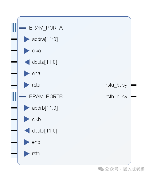
IP Core Instantiation Code (dual_port_rom_ip.v):
module dual_port_rom_ip( // Port A signals input clk_a, // Port A synchronous read clock (100MHz) input rst_n_a, // Port A active low reset (reset dout_a to zero) input en_a, // Port A read enable (active high) input [11:0] addr_a, // Port A read address (12 bits, 0~4095) output [11:0] dout_a, // Port A read data (12 bits) // Port B signals input clk_b, // Port B synchronous read clock (100MHz) input rst_n_b, // Port B active low reset (reset dout_b to zero) input en_b, // Port B read enable (active high) input [11:0] addr_b, // Port B read address (12 bits, 0~4095) output [11:0] dout_b // Port B read data (12 bits); // Internal reset busy signals (no need to expose, only complete port connections)wire rsta_busy;wire rstb_busy; // Instantiate Xilinx true dual-port ROM IP coreblk_mem_gen_0 u_blk_mem_gen_0( // Port A mapping .clka (clk_a), // Port A clock .rsta (~rst_n_a), // IP core reset active high, inverted to adapt to external active low reset .ena (en_a), // Port A read enable .addra (addr_a), // Port A read address .douta (dout_a), // Port A read data output .rsta_busy(rsta_busy), // Port A reset busy signal (internal) // Port B mapping .clkb (clk_b), // Port B clock .rstb (~rst_n_b), // IP core reset active high, inverted to adapt to external active low reset .enb (en_b), // Port B read enable .addrb (addr_b), // Port B read address .doutb (dout_b), // Port B read data output .rstb_busy(rstb_busy) // Port B reset busy signal (internal);endmodule
Top-Level Call File (top_dual_port_rom.v):
module top_dual_port_rom( input clk, // 100MHz clock input (shared by ports A/B) input rst_n // Active low reset input (shared by ports A/B)); // Internal signal definitions (Port A)reg en_a; // Port A read enablereg [11:0] addr_a; // Port A read address (12 bits, 0~4095)wire [11:0] dout_a; // Port A read data (12 bits) // Internal signal definitions (Port B)reg en_b; // Port B read enablereg [11:0] addr_b; // Port B read address (12 bits, 0~4095)wire [11:0] dout_b; // Port B read data (12 bits) // Instantiate dual-port ROM IP core encapsulation module (A/B ports share clk and rst_n)dual_port_rom_ip u_dual_port_rom_ip( // Port A connection .clk_a (clk), .rst_n_a (rst_n), .en_a (en_a), .addr_a (addr_a), .dout_a (dout_a), // Port B connection .clk_b (clk), .rst_n_b (rst_n), .en_b (en_b), .addr_b (addr_b), .dout_b (dout_b)); // Port A test logic: cyclically read addresses 0~4095always @(posedge clk or negedge rst_n) begin if(!rst_n) begin en_a <= 1'b0; // Disable read enable on reset addr_a <= 12'd0; // Reset Port A address to zero end else begin en_a <= 1'b1; // Continuously enable Port A read operation after reset release // Address cycles: reset to 0 after reaching 4095, otherwise increment addr_a <= (addr_a == 12'd4095) ? 12'd0 : addr_a + 1'b1; endend // Port B test logic: cyclically read addresses 0~4095 (independent but identical logic to Port A)always @(posedge clk or negedge rst_n) begin if(!rst_n) begin en_b <= 1'b0; // Disable read enable on reset addr_b <= 12'd0; // Reset Port B address to zero end else begin en_b <= 1'b1; // Continuously enable Port B read operation after reset release // Address cycles: reset to 0 after reaching 4095, otherwise increment addr_b <= (addr_b == 12'd4095) ? 12'd0 : addr_b + 1'b1; endendendmoduleTiming Constraints:
create_clock -name clk -period 10.000 -waveform {0.000 5.000} [get_ports clk] # -------------------------- Pin location constraints --------------------------# Clock pin: L5 (shared by dual ports A/B)set_property PACKAGE_PIN L5 [get_ports clk]# Reset pin: H5 (shared by dual ports A/B)set_property PACKAGE_PIN H5 [get_ports rst_n] # -------------------------- IO level standard constraints --------------------------# clk/rst_n use LVCMOS33 (3.3V), adapted to FPGA general IO voltage specificationsset_property IOSTANDARD LVCMOS33 [get_ports {clk rst_n}] # -------------------------- Auxiliary constraints --------------------------# Disable pull-up resistors on unused pins, reduce FPGA static power consumptionset_property PULLUP false [get_ports *]# Configure FPGA core voltage to 3.3V, matching IO level standardset_property CONFIG.VOLTAGE 3.3 [current_design] # -------------------------- ROM timing optimization constraints --------------------------# Constrain Port A address to data delay, ensure timing convergence under 100MHz clockset_max_delay 9.0 -from [get_ports addr_a] -to [get_ports dout_a] # Constrain Port B address to data delay, consistent with Port A set_max_delay 9.0 -from [get_ports addr_b] -to [get_ports dout_b]RTL Simulation Test File:
`timescale 1ns/1ps module tb_dual_port_rom; // Simulation signal definitionsreg clk; // 100MHz simulation clock (shared by dual ports)reg rst_n; // Active low simulation reset (shared by dual ports) // Port A observation signalwire [11:0] dout_a; // Port A read datawire [11:0] dbg_addr_a; // Port A read addresswire dbg_en_a; // Port A read enable // Port B observation signalwire [11:0] dout_b; // Port B read datawire [11:0] dbg_addr_b; // Port B read addresswire dbg_en_b; // Port B read enable /** * 100MHz clock generation: period 10ns (5ns high, 5ns low) * Forever loop flip, matching FPGA hardware clock frequency */initial begin clk = 1'b0; // Initial clock low forever #5 clk = ~clk;end /** * Reset signal control: * - 0~20ns: reset valid (low), initialize all registers * - 20ns after: reset release, start dual-port cyclic read logic * - 45000ns: end simulation (covering one round of reading addresses 0~4095, total 4096 cycles = 40960ns) */initial begin rst_n = 1'b0; // Initial reset valid #20 rst_n = 1'b1; // Release reset after 20ns #45000 $stop; // Stop simulation at 45020ns, ensuring complete observation of cycleend // Instantiate dual-port ROM top-level test moduletop_dual_port_rom u_top_dual_port_rom( .clk (clk), .rst_n (rst_n)); // Export debug signals (for simulation waveform observation) // Port A debug signalsassign dbg_addr_a = u_top_dual_port_rom.addr_a;assign dbg_en_a = u_top_dual_port_rom.en_a; // Port B debug signalsassign dbg_addr_b = u_top_dual_port_rom.addr_b;assign dbg_en_b = u_top_dual_port_rom.en_b; // Simulation print (optional): print dual port addresses and data every 100 cycles for quick verificationinitial begin $monitor("Time = %0t ns | PortA: Addr=%0d, Dout=%0d | PortB: Addr=%0d, Dout=%0d", $time, dbg_addr_a, dout_a, dbg_addr_b, dout_b);endendmoduleRun Results:
In the RTL simulation, the reset signal remains low valid from 0 to 20ns, with both Port A/B read enables set to 0, addresses cleared, and read data as 0; after the reset is released at 20ns, both ports’ read enables are immediately set to 1, and addresses increment from 0 each clock cycle, resetting to 0 after reaching 4095 and cycling; throughout the simulation period, the read data from ports A/B strictly matches their respective addresses (address N corresponds to data N, range 0~4095).

04
—
Summary
The Block Memory Generator IP core is an efficient way to implement BRAM in Xilinx FPGA development. Through visual configuration, different types of BRAM logic can be quickly generated, avoiding the timing risks of manually writing storage arrays. This article’s cases, based on the XC7Z015 platform, cover the full process of IP core configuration, instantiation, and verification for single/dual-port RAM/ROM, with code compatible with Verilog 95 standards, allowing for direct transplantation into actual projects; during development, it is necessary to select the BRAM type according to the application scenario, reasonably configure bit width/depth and initialization files, and combine timing constraints to ensure stability under a 100MHz clock, maximizing the advantages of BRAM hard resources.
Previous Articles:
FPGA RGB to HDMI Display Case
FPGA I2C Communication Example
FPGA SPI Communication Example
FPGA Serial Communication Example
Low Power Design Methods in Verilog
Common Hardware Implementations and Principles in Verilog
Synchronous FIFO and Asynchronous FIFO
Verilog Clock Division
Verilog Reset Design
FPGA Cross-Clock Domain Design