FPGA can often deter beginners due to the dual pressures of learning barriers and the cost of development boards.
Entry-level FPGA development boards on the market are not cheap; for instance, the classic Artix-7 series basic model costs several hundred RMB.
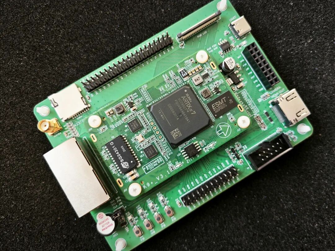
Recently, I stumbled upon a core board from a disassembled display screen image receiver card on a second-hand platform. The core is the XC7A50T—28nm process, 50K logic cells. The seller also developed a supporting baseboard to fully utilize the performance of the disassembled core board. The board includes basic components such as LEDs, buttons, Ethernet, HDMI, etc., and has reserved expansion interfaces, making it convenient for future projects involving sensors, cameras, and displays. It is very suitable for beginners in FPGA learning, and the key point is its very affordable price of only 135 RMB, which is much cheaper than a brand new development board. For those just starting with FPGA and wanting to practice basic logic circuits and Verilog syntax, this board, which balances performance, expandability, and cost-effectiveness, is indeed a reliable choice when paired with a downloader.
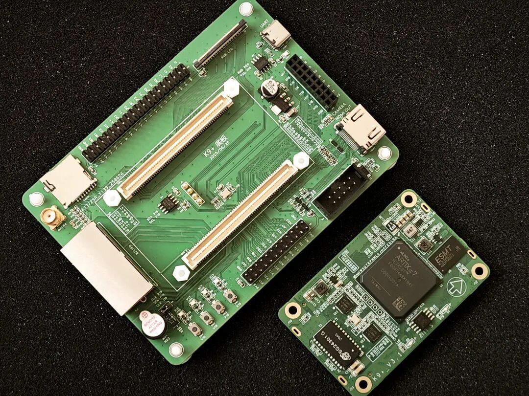
Those in the know understand that this type of disassembled FPGA development board hides “treasures.” Today, I will share my tips for finding such deals and my learning experiences, discussing the specific configurations and functionalities of this board.
1. Core Board Hardware Resources
First, let me clarify that this core board has a unique origin; it was disassembled from a display control board of a certain brand.
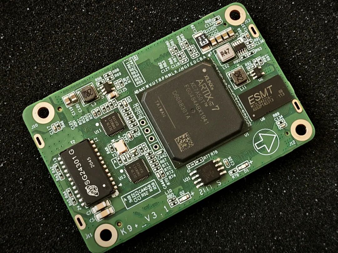
Despite its “second-hand” status, the hardware configuration is quite impressive. The core is Xilinx’s XC7A50T, and the board is equipped with essential components such as a network card, memory, and storage. Let’s go through them one by one.
The core chip is the Xilinx Artix-7 series XC7A50T, which is a mid-range model with a 28nm process and 52K logic cells.
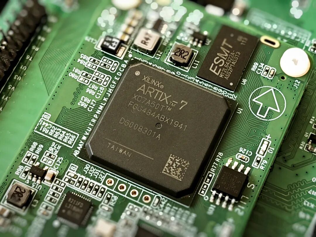
This scale is just right for beginners; it won’t waste resources due to being too “luxurious,” nor will it be too “meager” to handle basic projects, making it a “golden configuration for beginners.”
What is most surprising is the network card configuration, which actually includes two Realtek RTL8211 gigabit network cards with RGMII interfaces.
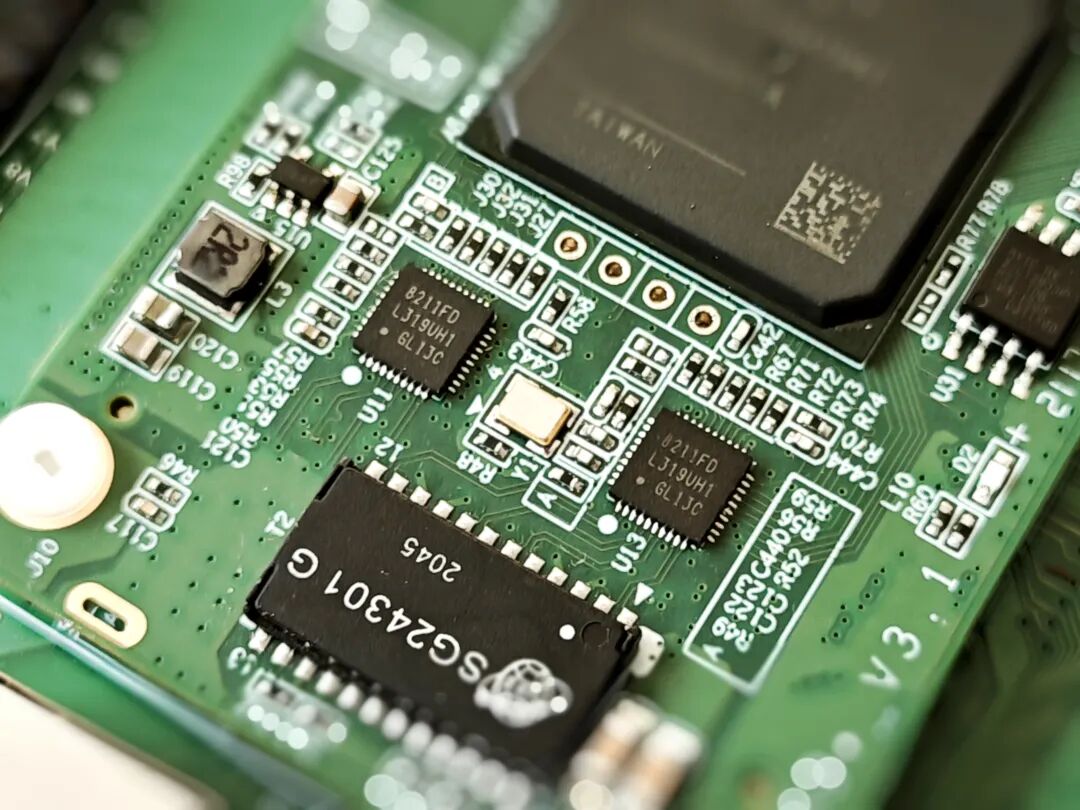
These two “brothers” share a single 25M active crystal oscillator and are thoughtfully assigned different physical addresses, one at 0x1 and the other at 0x2, preventing conflicts during debugging.
By the way, the FPGA’s clock also comes from the CLKOUT pin of one of the network cards, at a frequency of 25M.
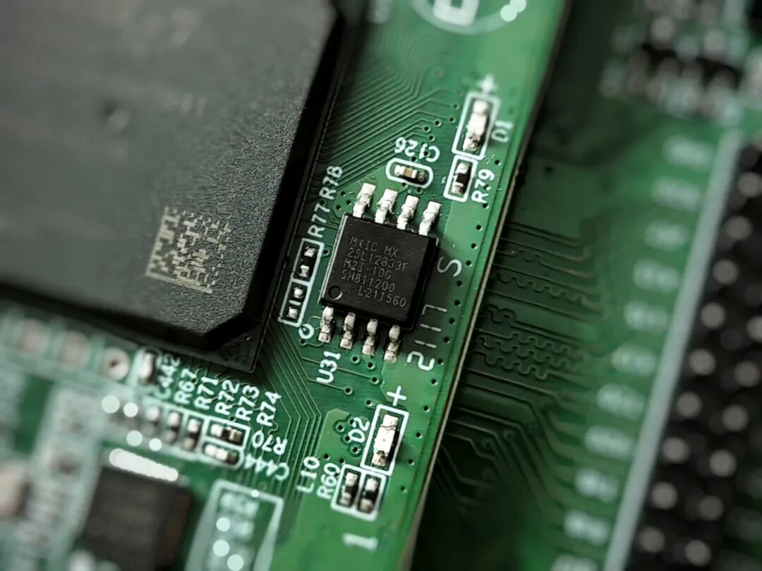
The storage and memory are also sufficient; the storage chip is Macronix’s MX25L128, with a single-line SPI interface and 128Mb (16MB) of space, which is more than enough for storing programs and configuration files.
The memory used is ESMT’s M12L64322A, a 64Mb (8MB) SDRAM, which is more than enough for caching image data, ensuring that beginners won’t experience any bottlenecks.
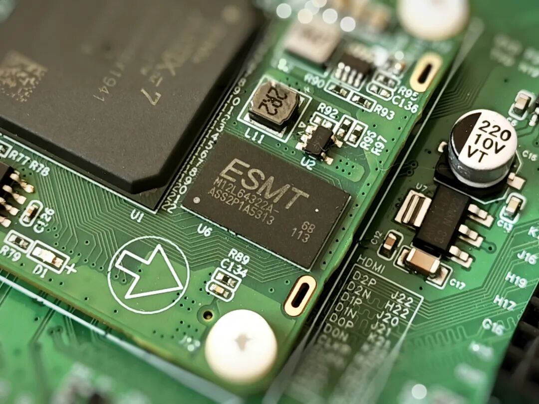
The power supply is also very user-friendly, requiring only a single 5V supply. The onboard DC/DC and LDO will automatically convert to 3.3V, 1.8V, and 1.0V, the voltages required by the chips, eliminating the need for us to mess around with the power circuit, which is very friendly for beginners.
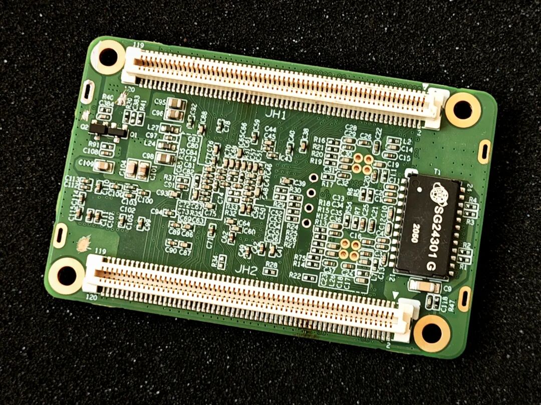
Other details are also well thought out: two SG24301G network transformers, with signals directly routed through board-to-board connectors, allowing for easy connection of a network port socket.
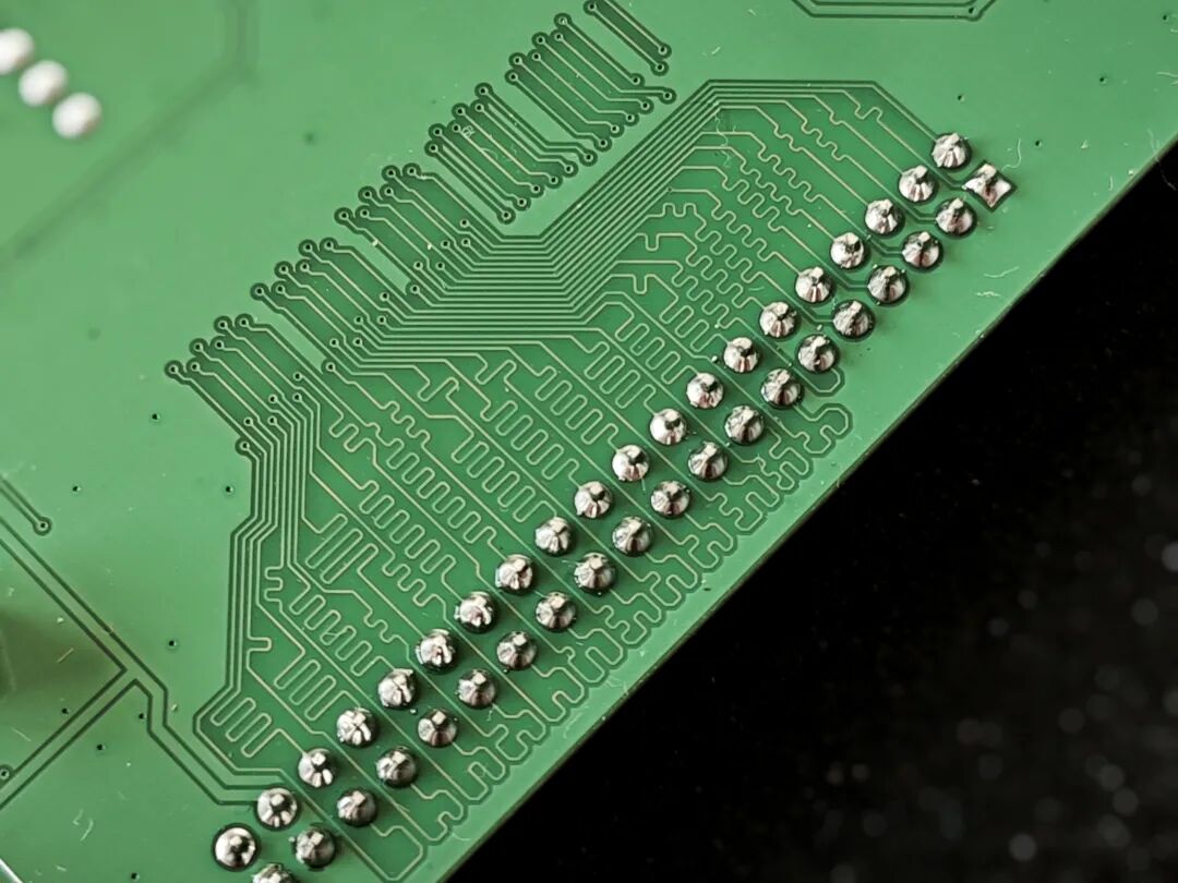
The JTAG interface is located in the center of the board, using a standard 4P 2.54mm pin header, which can be directly connected to a debugger for testing. Externally, there are two 120Pin 0.8mm pitch board-to-board connectors, providing ample expansion capability.
There are also two LEDs; the red one is the power indicator, which lights up when powered on; the green one is the user LED, which lights up at low level, perfect for practicing the simplest IO control or breathing light effects, serving as the first lesson for beginners.
Overall, the resources on this board are “sufficient and considerate.” There are no flashy extra configurations, but all core components such as storage, memory, and network cards are present, and all exposed pins are at 3.3V level standards, so there is no worry about damaging components.
Now let’s take a look at the resources on the baseboard.
2. Baseboard Hardware Resources
The expansion resources on the baseboard are quite rich, fully meeting the learning needs from beginner to advanced levels.
It is equipped with two network port sockets, supporting gigabit rates, which are just right for practicing FPGA implementations of protocols such as MDIO, ARP, ICMP, UDP, and for conducting high-speed communication experiments with computers.
The board also includes one active buzzer, which can be controlled with a jumper cap; it can be disconnected when not in use to prevent “random sounds”;
Four user LEDs and four tactile buttons are all active at low level, making them perfect for basic IO control experiments.
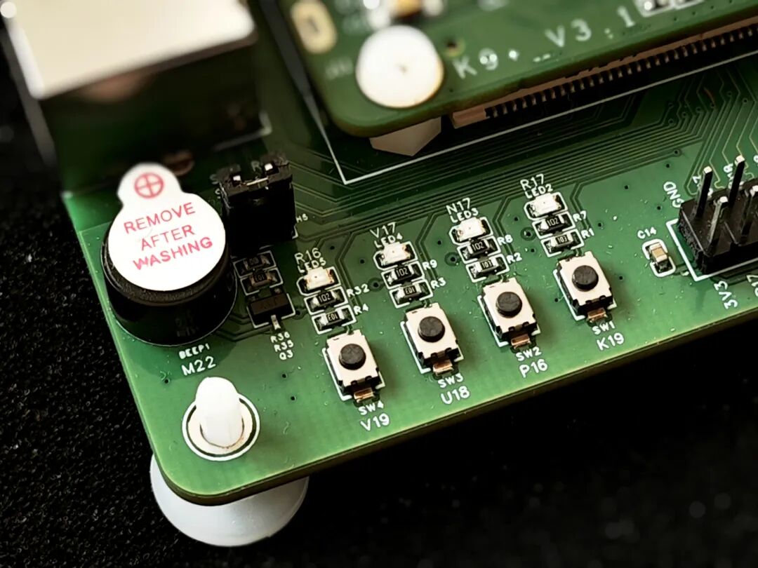
Clock and storage expansion have also been considered: one 50M active crystal oscillator is directly connected to the FPGA’s global clock pin, providing a stable clock source for high-speed experiments;
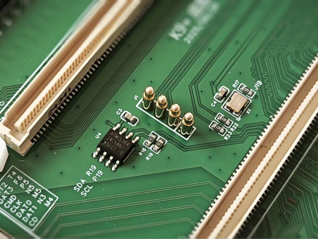
One 24C64 EEPROM chip is just right for learning IIC interface communication.
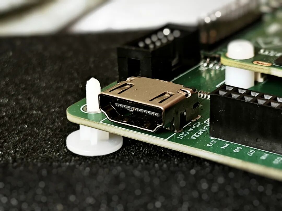
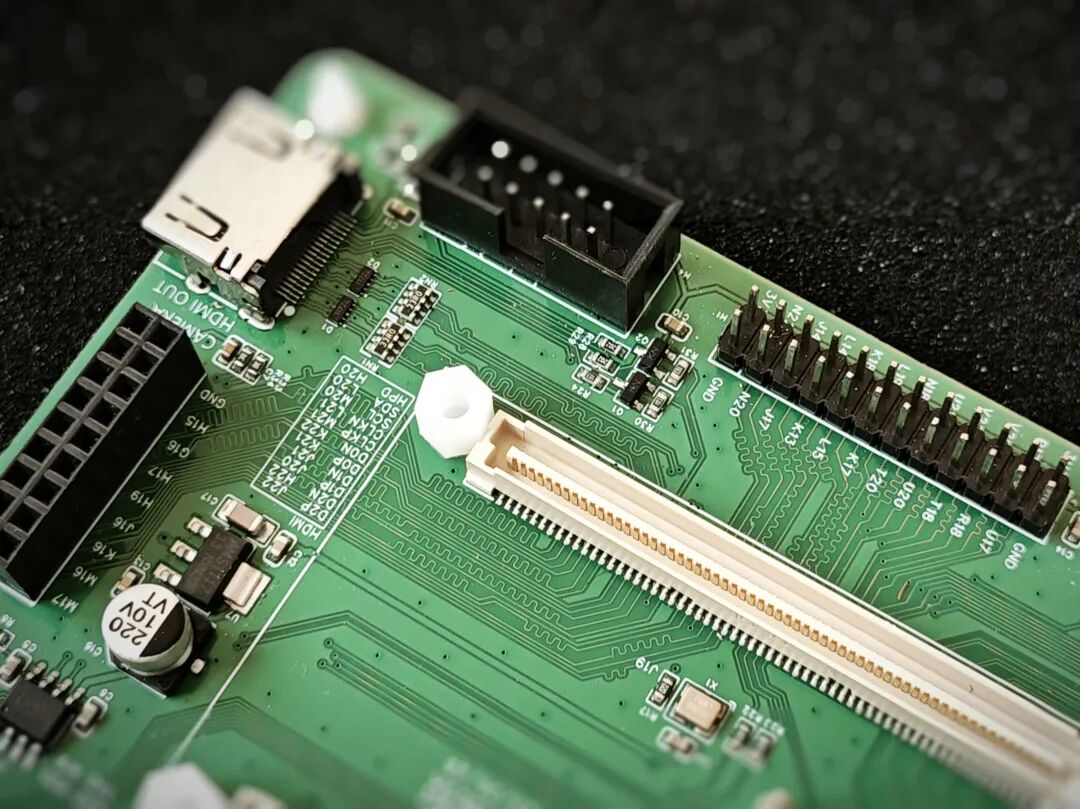
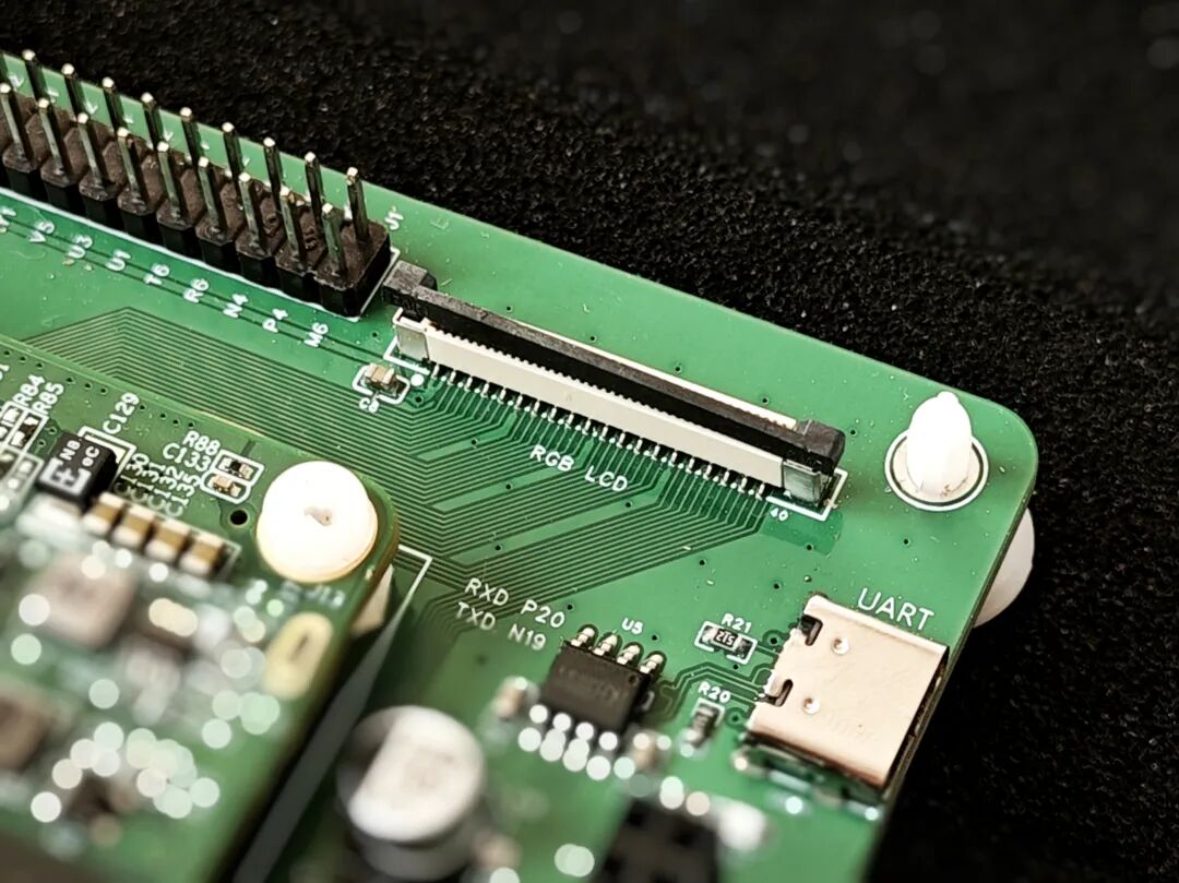
The display and image acquisition parts are highlights; not only does it have an RGB LCD interface supporting RGB888 LCD screens, but it also has a complete standard HDMI-A interface—capable of using FPGA to implement TMDS encoding for image output, and can read the model, resolution, and other parameters of the display using the IIC protocol; paired with a 2*9P camera interface, it can directly connect to modules like OV7725 and OV5640 for image acquisition projects.
The storage and debugging interfaces are also very considerate: a standard 7-pin SD card socket supports both SDIO and SPI driving modes, and includes insertion detection functionality;
The CH340N serial chip paired with a Type-C interface forms a debugging serial port, making it very convenient to connect to a computer.
For expansion, the 40PIN interface can directly connect to modules like AD/DA from Zedboard.
One SMA interface is directly connected to the FPGA pins, with low loss for coaxial cable, suitable for long-distance transmission of high-speed signals.
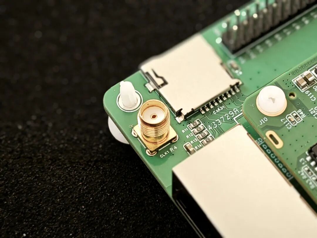
Other unused signals are routed through a 2*12P standard pin header, making it easy to connect custom modules.
For debugging, a standard 10Pin JTAG interface is provided to meet programming download and debugging needs.
It is worth mentioning that the design of the JTAG interface connection on the baseboard is quite clever. The JTAG interface of the core board is independently routed through pin headers, rather than through the board-to-board connector. How can we smoothly connect it to the baseboard’s download socket? The conventional approach is to use pin headers and female headers to connect, but this combination’s height far exceeds that of the board-to-board connector, making it cumbersome to plug and unplug, which can be somewhat counterproductive.
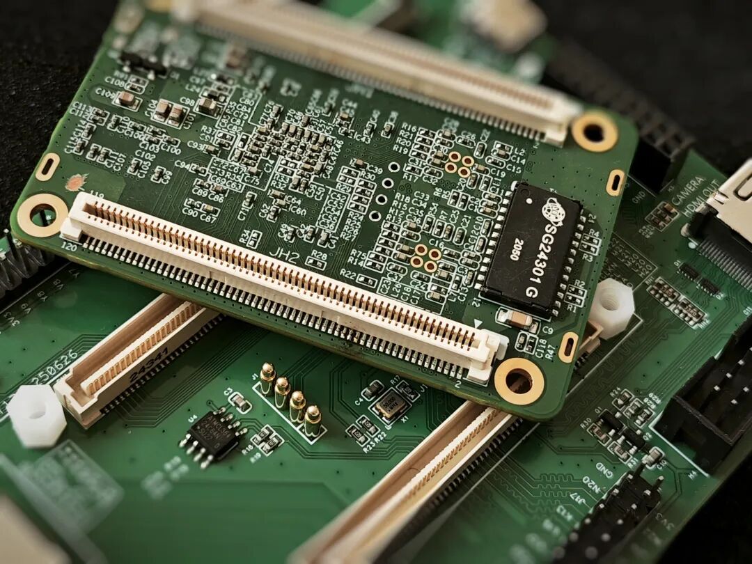
The solution on the baseboard is very ingenious: four short spring-loaded pins are soldered in the corresponding positions. With precise length selection, when the core board is engaged, the pins can make stable contact to achieve signal conduction, ensuring stability; and when the core board needs to be unplugged, the compressed structure of the pins does not cause any obstruction, allowing for smooth insertion and removal. This design does not use any complex technology but balances the needs for “stability” and “convenience” perfectly, and it must be said that the designer has indeed put thought into it.
3. Supporting Documentation
It should be noted that this core board comes from disassembled equipment circulating in the market, so the original factory schematic for the core board cannot be provided. However, the core FPGA pin definitions have been fully obtained, which can fully meet development and debugging needs, providing core support for hardware development.
The most considerate part is the accompanying FPGA learning examples, most of which have been ported from established development board manufacturers like Zedboard and Black Gold, ensuring stability.
The content covers everything from “beginner to practical application,” including essential projects for beginners such as LED lighting and button filtering, as well as advanced storage control experiments like EPROM reading and writing, and SDRAM operations; in terms of display, examples for VGA and HDMI displays are all provided, and even practical projects close to real applications, such as “LCD display camera images” and “UDP transmission of camera images,” are included.
If you want to delve deeper into embedded systems, advanced MicroBlaze learning examples are also included, providing a set of examples that can support learning needs from beginner to advanced, eliminating the need to search for resources elsewhere.
In summary, although the core board lacks the original factory schematic, the key documentation and learning resources are well provided. For beginners, these materials are sufficient to support the entire learning process from basic experiments to practical projects.
Conclusion
This development board provides a complete progression path for FPGA learning. In the beginner stage, one can master basic peripheral operations such as LED driving, button filtering, and buzzer control, as well as implement common communication protocols like IIC, SPI, and UART, while completing design practices for storage units like FIFO and RAM; in the advanced stage, one can delve into complex application development such as RGB display driving, HDMI TMDS encoding, camera data acquisition, and SDRAM read/write control; in the high-level stage, one can engage in MicroBlaze soft core development. If one has experience with microcontrollers like STM32, learning the soft core will be easier, and it can also run the FreeRTOS real-time operating system, mastering peripheral management such as GPIO, serial ports, timers, and interrupts, as well as communication methods between the soft core and FPGA logic based on shared BRAM and AXI protocols, achieving firmware online upgrade functions similar to microcontrollers, and constructing multi-image boot schemes based on MultiBoot and ICAP technology.
This development board also supports a wealth of expansion applications: when paired with a CAN transceiver module, CAN protocol communication can be achieved through pure logic or soft core; based on its hardware resources, advanced practices such as zip/LZMA data compression, JPEG/MPEG image encoding and decoding, floating-point operations, and SHA encryption algorithms can also be conducted. Additionally, it allows for high-level synthesis (HLS) technology learning, converting C language functions into FPGA callable IP cores for custom function development, such as basic machine vision applications like image edge detection.
It should be noted that the storage chip on the core board is SDRAM rather than DDR, so the soft core cannot run large programs like the LwIP protocol stack, which is a shortcoming in the hardware configuration of this development board.