Name: Design of FPGA-based FIR Digital Filter Verilog Code and Quartus Simulation
Software: Quartus
Language: Verilog
Code Function: Design and implement a digital filter based on FPGA using the knowledge acquired.
The circuit device is described using VHDL, implementing the design of the FIR filter based on FPGA. Master the principles of FIR filters, basic network structures, and common implementation methods of FIR filters. Determine the design scheme of the FIR filter, overall design ideas, algorithm decomposition, coefficient extraction, and solve some key issues.
Design Document:
Filter Parameters
Sampling Rate f_s = 100kHz, design cutoff frequency of 10KHz for the FIR filter.
The designed filter is 7th order (length 8), input in Matlab: fir1(7, 0.2);
Its normalized cutoff frequency is 0.2 (corresponding to the actual frequency of 0.2 * f_s/2, where f_s is the sampling frequency)
|
Parameter |
Value/Description |
|
Sampling Rate f_s |
100 kHz |
|
Window Function Type |
Hamming Window |
|
Normalized W_n |
0.2 |
|
Actual Cutoff Frequency f_c |
10 kHz |
|
Nyquist Frequency |
50 kHz (f_s/2) |
Parameter Design Method:
Use Matlab software to design filter coefficients
Filter Coefficient Design:
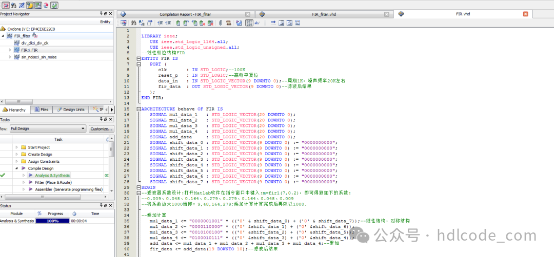
Open Matlab software and type in the command window: m=fir1(7,0.2), to obtain the following coefficients:
0.009, 0.048, 0.164, 0.279, 0.279, 0.164, 0.048, 0.009
Scale the coefficients by 1000, i.e.: 9, 48, 164, 279; after performing the multiplication and addition calculations, divide by 1000.
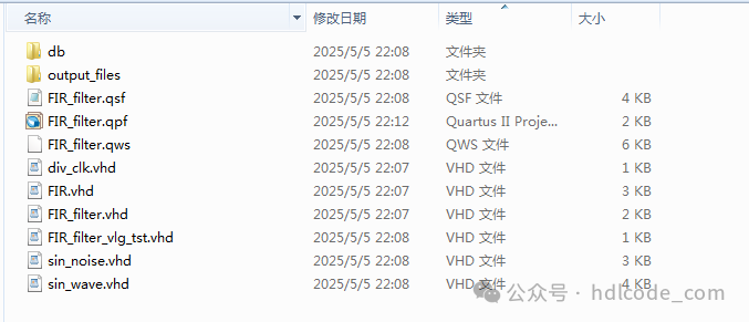
1、Project Files
2、Program Files
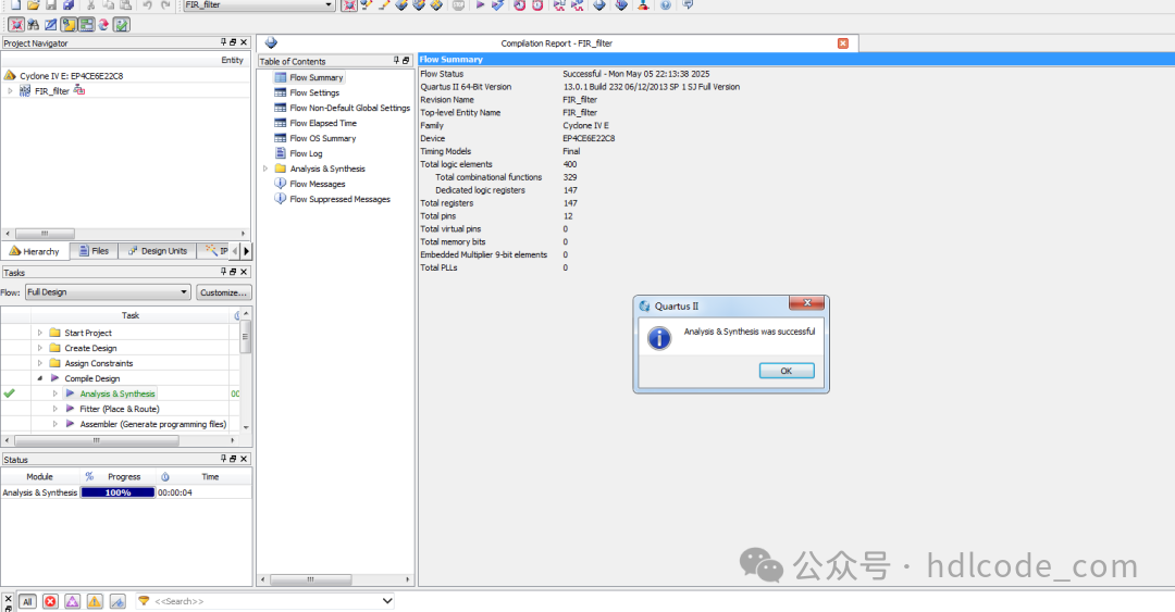
3、Program Compilation
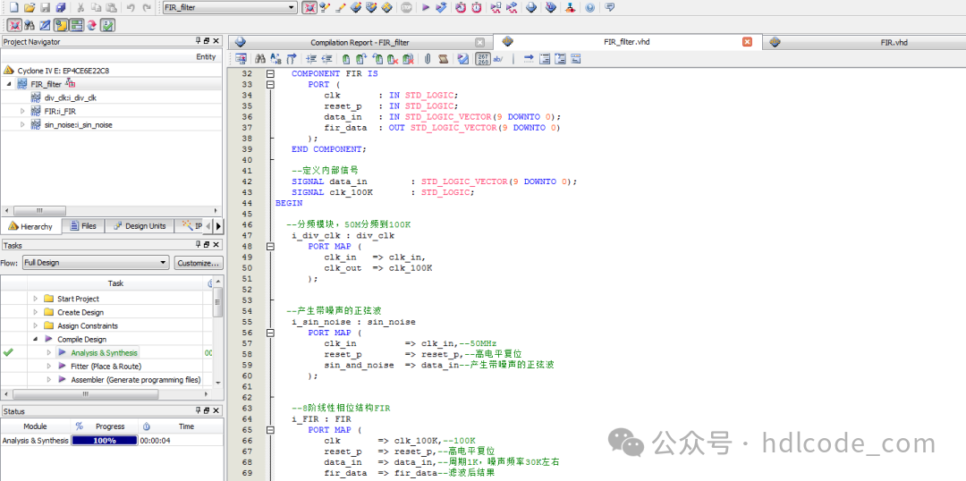
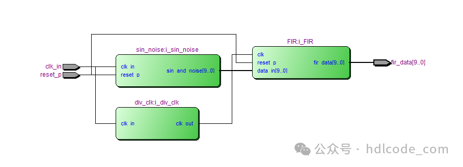
4、RTL Diagram
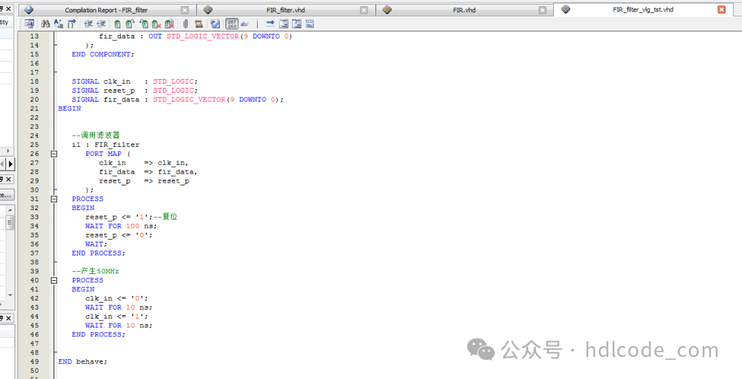
5、Testbench
6、Simulation Diagram
Overall Simulation Diagram
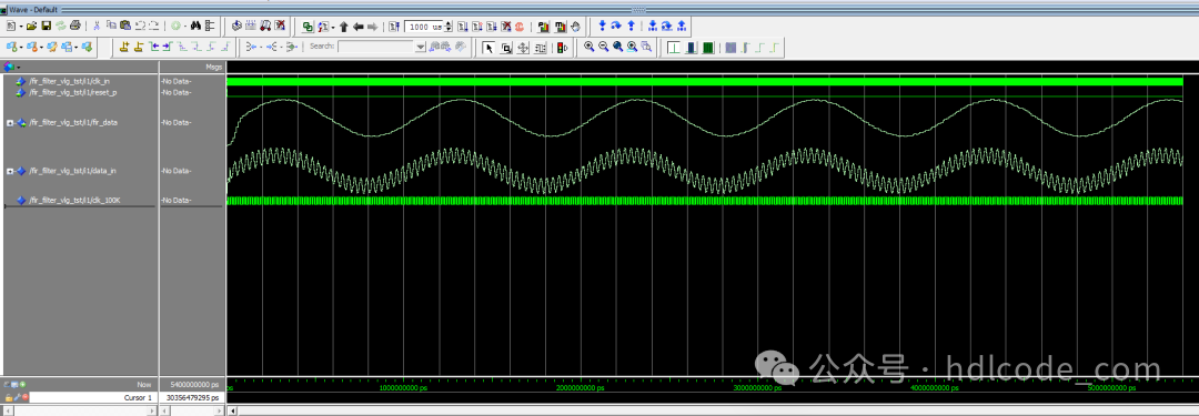
In the above figure, data_in is the test signal composed of the superposition of 30KHz and 1KHz sine wave signals, and the output fir_data is the filtered signal. It can be seen that the 30KHz signal is filtered out while the 1KHz signal is retained, verifying the functionality.
Frequency Division Module

Frequency division generates a 100Hz sampling signal
FIR Filter Module
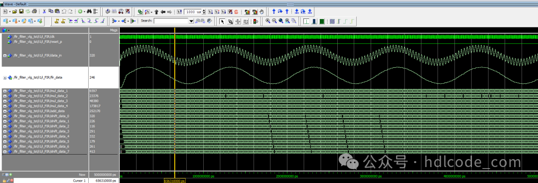
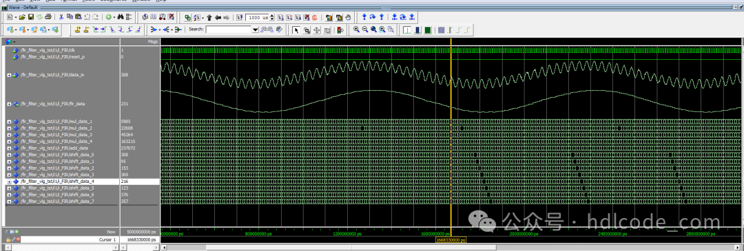
In the above figure, data_in is the test signal composed of the superposition of 30KHz and 1KHz sine wave signals, and the output fir_data is the filtered signal. It can be seen that the 30KHz signal is filtered out while the 1KHz signal is retained, verifying the functionality.
Noise Test Signal Generation Module
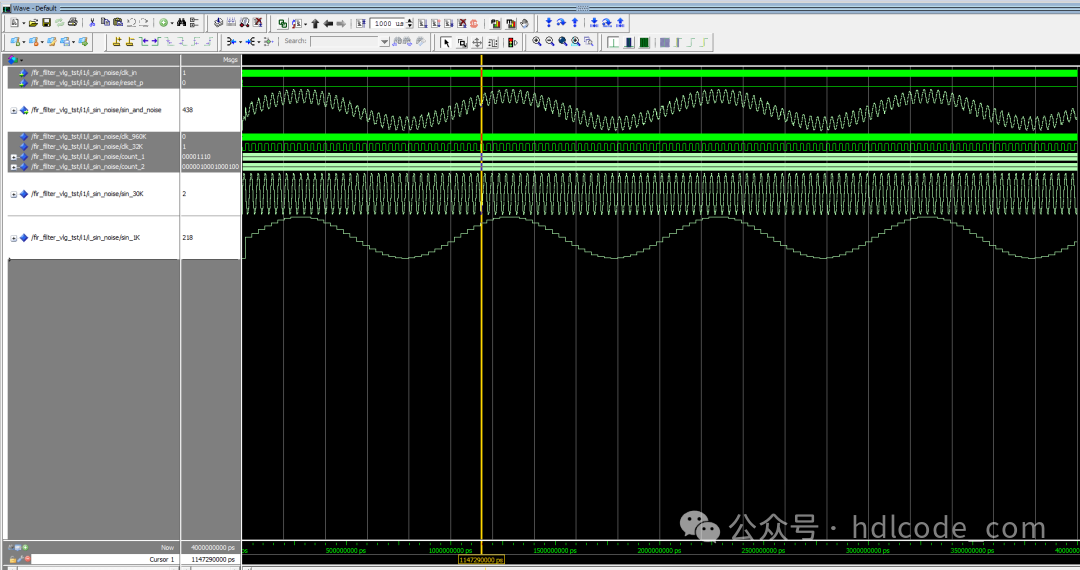
In the above figure, sin_30K is the 30KHz sine wave, sin_1K is the 1KHz sine wave, and the two waveforms are superimposed to obtain the sin_and_noise signal, which is used to test the filter functionality.
Partial Code Display:
LIBRARY ieee;
USE ieee.std_logic_1164.all;
USE ieee.std_logic_unsigned.all;
–Frequency division module, dividing 50M to 100K, as the sampling signal
ENTITY div_clk IS
PORT (
clk_in : IN STD_LOGIC;
clk_out : OUT STD_LOGIC
);
END div_clk;
ARCHITECTURE behave OF div_clk IS
SIGNAL count : STD_LOGIC_VECTOR(15 DOWNTO 0) := “0000000000000000”;
BEGIN
PROCESS (clk_in)
BEGIN
IF (clk_in’EVENT AND clk_in = ‘1’) THEN
IF (count >= “0000000111110100”) THEN–50_000K/100K=500
count <= “0000000000000000”;
ELSE
count <= count + “0000000000000001”;
END IF;
END IF;
END PROCESS;
Code file (paid download):