PCB Network City News
Today, we share a summary of experiences in PCB process design, hoping to inspire industry colleagues.1 PCB Basic Technology
1.1 PCB Size and Shape
The welding processing dimensions of PCB materials are width (200mm~250mm) * length (250mm~300mm).For PCBs with a long edge less than 125mm or a short edge less than 100mm, a panelized approach can be used (as shown in Figure 1).This size helps avoid issues during wave soldering and reflow soldering processes.If the shape is not rectangular, it may cause instability during processing on the conveyor belt, flipping during insertion, and solder splashing onto component surfaces when passing through the wave soldering tank.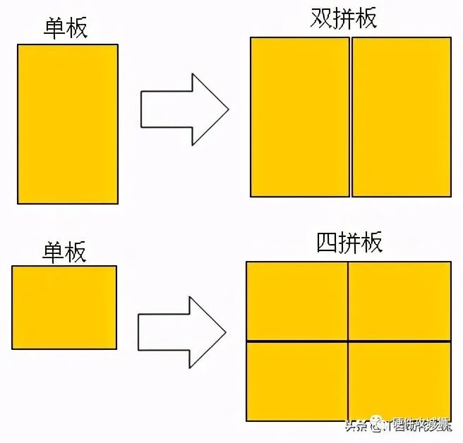 Figure 1If not rectangular, use a process panel to assemble irregularly shaped PCBs into a rectangle, especially if there are notches in the four corners, which should be filled to form a rectangle;for PCBs with only surface-mounted components, notches are allowed, but the notch size must be less than 1/3 of the length of the edge.
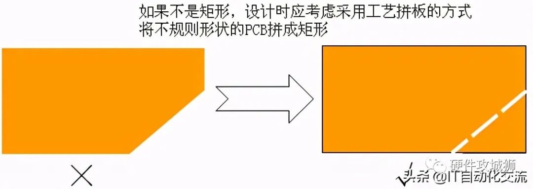 Figure 2
1.2 PCB Substrate
In the design of the circuit board, the requirements for PCB materials must be specified and marked in the technical requirements of the PCB design documents, including:PCB material and grade (commonly used are epoxy resin glass fiber cloth-based FR-4, FR-5);flame retardant grade (UL94-V0, UL94-V1 level or green flame retardant type);material thickness, nominal specifications are 0.8, 1.0, 1.2, 1.6, 2.0, 2.5, 3.0, 3.5 (unit mm);material thickness tolerance ±10%;for medical device products, the material thickness must be ≥1.6mm, A1, A2 grade;for instruments used in flammable and explosive environments, the flame retardant grade should be marked on the PCB.
1.3 Coating
PCB coating types include tin plating (preferred), nickel-gold plating. Tin-plated PCBs are prone to oxidation when exposed to air for long periods,and should be vacuum packed during storage in the factory.
1.4 Number of Layers
Multi-layer PCBs have outstanding performance in electromagnetic compatibility protection,but also have higher manufacturing costs,so the design should compromise based on signal requirements.When fclk>5MHz or tr<5ns (the rise or fall time of the pulse), multi-layer boards are recommended;once multi-layer boards are determined, the number of routing layers should be based on pin density.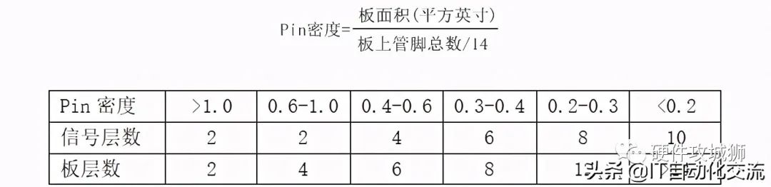 Figure 3 Pin DensityIf a double-sided board is necessary, one side of the PCB must be made as a complete ground layer.
1.5 Design for Manufacturability
When designing PCBs, it is essential to leave space and reference for the production process to avoid technical hazards during production.During assembly and soldering, the edges of the PCB should leave ≥5~10mm of blank width, without placing components or solder points, as process edges.If the PCB cannot leave process edges, auxiliary edges of 5~10mm can be added to both conveyor edges as process edges, which can be removed after soldering.Reference points used during the assembly process (also known as optical MARK points) must be set on the PCB as reference points for component placement,and the pad form and symmetrical layout of the reference points should be confirmed with the process engineers of the assembly factory.A background area should be created around the MARK points, and no other pads, silkscreen, or solder mask should be present in this area.The center of the reference point should be more than 5mm from the board edge; at least two of each type of reference point should be set in diagonal and asymmetrical positions.BGA and multi-pin packages should have local reference points to prevent thermal errors during operation or cumulative errors of the PCB, which may cause misalignment of fine-pitch component placements.For BGA packaged devices and other packaged devices with pin counts ≥100, a pair of local reference points must be placed diagonally;optical reference points should be placed within 5mm of the device perimeter;no components should be placed within 3mm of the optical reference points.
2. Pads and Vias
2.1 Pads
The quality of pads directly affects the soldering effect, so the design of pads is crucial.When the pad hole diameter is 0.3~0.5mm wider than the device lead,and the total pad diameter is 2~2.5 times the pad through hole diameter,these are ideal conditions for achieving good wetting angles during soldering.Through-hole pads for through-hole resistors, capacitors, inductors, ferrite beads, diodes, and transistors should have a hole diameter D = outer diameter d of the component lead + (0.3~0.5mm).Surface mount pads at both ends should be well-symmetrical to ensure the surface tension of the molten solder is balanced, avoiding solder bridges and displacements during soldering; violating this requirement may lead to soldering defects during reflow soldering.When there are many pins on each row of through-hole components, the pad arrangement direction should be parallel to the board entry direction; it is recommended to set solder pads to absorb excess solder, avoiding soldering of 2~3 pads parallel to the board entry direction at the tail end of the wave soldering.
2.2 Through Vias
Through via design rules: standard through via dimensions are:hole diameter:board thickness ≥ (1:6);for high-speed signals, a single via generates 1~4nH of inductance and 0.3~0.8pF of capacitance, and the number of vias should be minimized when routing high-speed signal lines; for parallel high-speed signals, such as address lines and data lines, if layer changes are unavoidable, ensure that the number of vias for parallel signal lines is the same.
2.3 Mounting Screw Holes
Mounting screws on the PCB should have a no-go area, with the no-go area diameter = (screw diameter * 2.2) + (2~3mm), to ensure sufficient electrical insulation space.
3. Layout Rules
3.1 Component Orientation
For through-hole components with multiple pins, such as connectors, DIP packaged devices, and T220 packaged devices, the layout should make their axes perpendicular to the wave soldering direction.Active components like PLCC and QFP should avoid wave soldering.Similar types of through-hole components should be placed in the same direction along the X or Y axis.For similar polarized discrete components, it is best to maintain consistent polarity direction within a functional area along the X or Y axis.
3.2 Component Layout
The recommended minimum spacing between components is:① The edge spacing between small surface-mounted resistors and capacitors should be >0.3~0.7mm;② The spacing between other surface-mounted components, SOTs, and between SOIC and surface-mounted components should be 1~1.25mm;③ The spacing between SOICs and between SOIC and QFPs should be 1.5~2.0mm;④ The spacing between PLCCs and surface-mounted components, and between SOIC and QFP should be 2~2.5mm;⑤ The spacing between PLCCs should be 3~4mm;⑥ The spacing between the outer side of through-hole component pads and the outer side of surface-mounted component pads should be greater than 1.5~2mm;⑦ The spacing between through-hole components during wave soldering should be greater than 1~2mm;⑧ The distance between BGA and adjacent components should be greater than 3~5mm.For adjustable and pluggable components, SMT components should not be placed within a 3mm range around the board surface to prevent insertion stress from damaging components;pluggable connectors far from mounting pillars should preferably be flat connectors.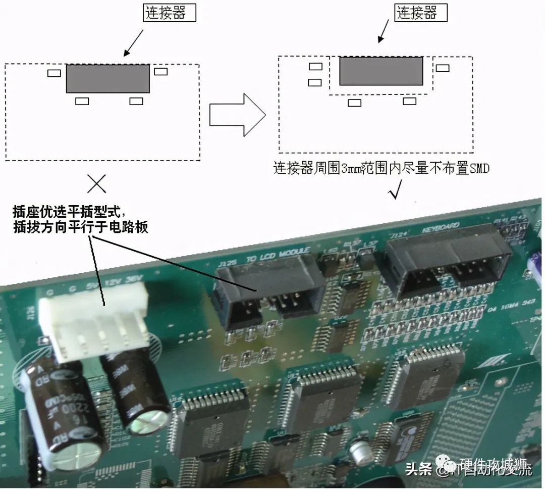 Figure 4 Socket Installation DirectionUnder natural cooling conditions, temperature-sensitive components, such as ceramic capacitors, electrolytic capacitors, thermistors, and temperature-sensitive ICs, should be kept away from heat-generating components;if they cannot be kept away, temperature testing should be conducted to ensure that the temperature rise of temperature-sensitive components is within the derating range.
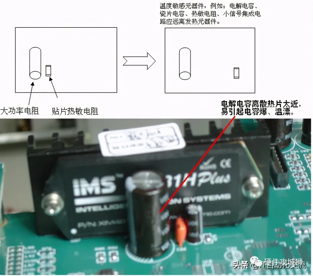 Figure 5 Temperature Sensitive Components Away from Heat SourcesLayout rules matching soldering processes:① To reduce the number of PCB heating cycles, the following order should be used to select component layout methods: single-sided through-hole — single-sided surface mount — single-sided mixed — A-side mixed B-side through-hole — A-side mixed B-side surface mount — double-sided mixed;② If there are a few components, such as buzzers, LEDs, sockets, etc., that must be inserted on the bottom side, manual rework can be used.Components with thermal power density >0.4W/cm3 should have heat sinks or be mounted on metal bases or enclosures to improve their overheating capability.High-power resistors without heat sinks should be elevated 3~5mm for heat dissipation.
4 Wiring Rules
4.1 PCB Wiring Coating
The relationship between PCB copper foil line width/thickness/current carrying capacity is determined according to (Figure 4.1):Printed conductors generate temperature rise due to current flow, which is related to the width of the conductor when the copper foil thickness is constant.If the design requires increasing the current of the conductor but cannot widen the conductor, the temperature rise of the conductor should be fully estimated.According to standard SJ/Z1675-81, when the thickness of the conductor is constant, the relationship between the load current and temperature rise for conductors of different widths is shown in the figure.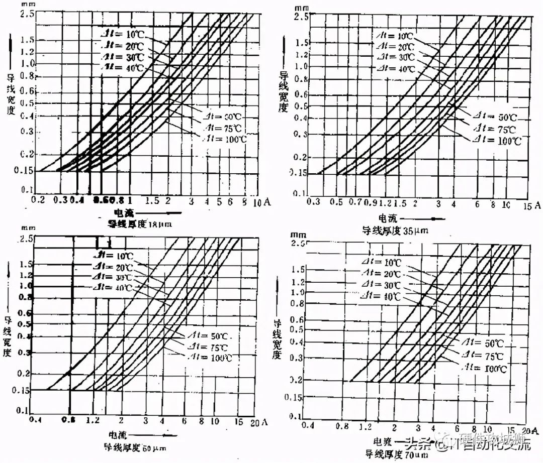 Figure 6
4.2 Wiring Rules
Gold fingers protruding from the board edges, the two ends of the board side where the gold fingers are located (R1.0~R1.5 rounded corners), and the insertion end face of the gold fingers (the chamfer size refers to the PCB thickness, R0.5 or less, to facilitate insertion and removal) should be chamfered;the inner end of the gold fingers should not have pads, and pads and components should be kept away from the gold fingers.A/D signals, input/output signals, signals with two orders of magnitude difference in current, high/low voltage, and high/low frequency signals must be kept away from each other; if they cannot be kept away, ground lines should be laid in between.The spacing between any lines should be ≥3 times the printed line width, i.e., ≥3W, to avoid 70% of the electric field interference between the two lines.The ground layer on the PCB should protrude 20H from the edge of the power layer and signal layer (the thickness of the power and ground or signal layer to ground is 1H), limiting 70% of the electric field radiation within the edge of the ground layer.A 3mm no-go area should be left around BGA devices, with the best being a 5mm no-go area.Signal lines should be avoided under crystal oscillators, heat sinks, relays, optocouplers, power modules, transformers, and voltage regulators.The wiring width within the same grid should remain consistent; variations in line width can lead to uneven impedance characteristics, causing reflections when the signal transmission speed is high, which should be avoided in PCB wiring. If line width variations cannot be avoided, the effective length of the inconsistent parts should be minimized, such as the lead lines of BGA packages and connectors.Signal lines and their return loops should form closed loops; floating wiring is not allowed on this closed loop; special attention should be paid to self-loops that may occur on the same or different layers, causing unnecessary radiation and receiving interference.Pads on large copper foils should be connected to pads through thermal pads, i.e., thermal pads, with connections between pads and copper foils in a “米” or “十” shape. Thermal pads should not be used for pads carrying large currents.
4.3 Socket Pin Routing
Each power line on the socket pin should be paired with at least one ground pin.
5 Marking
5.1 Marking Types
The following areas and contents on the PCB should be marked with silkscreen: PCB version number, pin symbols, component polarity, component orientation, safety markings, hazard markings, and parameter values of key points (e.g., marking the supply voltage next to the power socket, Vcc1 3.3V; marking the power voltage and parameters at the voltage pins of key ICs, and other functional parameters such as waveforms, frequencies, etc.).Warning identifiers should be in all capital letters, and descriptive text should start with a capital letter followed by lowercase letters.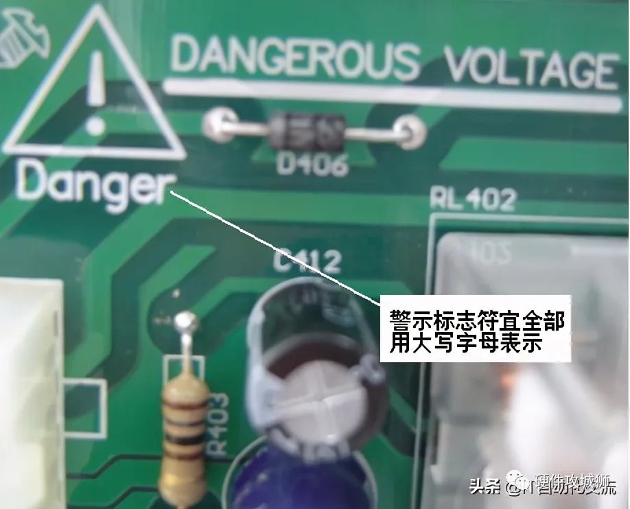 Figure 7 Marking RequirementsFuse markings should include fuse number, fusing characteristics, rated current value, explosion-proof characteristics, rated voltage value, English warning markings, etc. If there is no space on the PCB for layout markings, the warning content can be explained in the product manual.All five safety regulation markings on the PCB (certification marks, manufacturer, manufacturer model, certification document number, flame retardant grade) should be complete.
5.2 Marking Requirements
Silkscreen numbers should be placed next to the corresponding components and should not be covered by the components after installation or obscured by the body or other components; the orientation of numbers within each board should remain consistent, or consistent within a functional circuit range.No silkscreen should be present on pads, solder paths, vias, or test pads.Silkscreen should clearly indicate representative pin numbers for easy identification of other pins and checking the direction of connectors.The spacing between silkscreen characters should be >5mil, and the spacing from the edge of the pad should be >5mil; the width of silkscreen characters should be 6mil~12mil, with a recommendation of 8~10mil, and the height of silkscreen characters should be 50mil~60mil; adjustments can be made for smaller PCB areas.
6 Testability Design
ICT test points on the PCB should be on the soldering side; test point pad sizes should be ≥24mil (0.6mm), and the minimum spacing between two separate test points should be 60mils (1.5mm);For PCBs requiring ICT testing, two 125mil non-plated holes should be designed diagonally on the PCB for ICT test positioning;surface mount component pads should not double as test pads.When the machine is powered on, a digital multimeter can be used to check the total supply voltage of the board, the supply voltage of each functional circuit, the voltage of key components, and the waveforms at key points.When designing the PCB, these test pads should be set up and labeled with TP1, TP2, etc., with voltage values and test waveforms noted in the operation manual.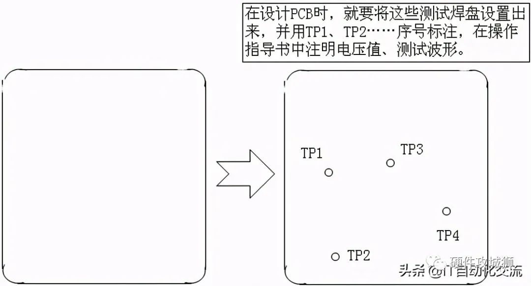 Figure 8 Test Point Requirements
7 Cables
Non-shielded signal wire twisting criteria:① Non-shielded signal cables should not be twisted together with incompatible signal wires (in/out, A/D signals, high/low level signals, high/low frequency signals);② The outgoing signal and return signal of the signal wire should be twisted together.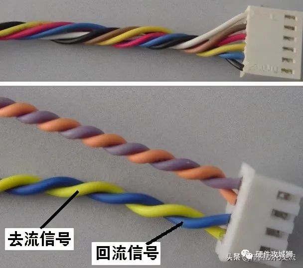 Figure 9 Outgoing and Return Signals Twisted TogetherOn shielded cables, magnetic rings should be installed on the inside of the shield layer.Magnetic rings on cables inside the chassis should be fixed to the circuit board or chassis wall with hot melt glue.
8 Board-Level Grounding Measures
For signals above 10MHz, multiple point grounding should be done nearby, with a large area of copper covering the ground layer.Grounding rules for mixed high and low frequency circuits:≤1MHz should use single-point grounding (but be cautious of common impedance interference);≥10MHz should use multiple point grounding nearby;for frequencies between 1~10MHz, if the ground line length < λ/20, then single-point grounding is used; if the ground line length > λ/20, then multiple point grounding is used; λ is the wavelength.It is recommended to separately ground low-frequency digital ground (below 10MHz), analog ground, working power ground (for relays, stepper motors), safety ground, surge protection ground, and shield ground,and then connect the grounds through direct connections, small resistors, magnetic beads, capacitors, and large resistors, with the specific connection method determined by the grounding purpose.The purposes of grounding are as follows:① If only ground is needed — ground equal potential, then direct connection;② If there are pulse currents on the digital ground but equal potential is needed for both grounds, then connect with a small resistor to slow down the ground current impact;③ If interference on the ground is relatively high frequency, use magnetic beads to dissipate high-frequency pulse currents;if static charge discharge is desired but DC isolation is needed, connect with a capacitor.Source: Hardware Engineer,Copyright belongs to the original author, the purpose of reprinting is to share more information, and does not represent the position of this account. If copyright issues arise, please contact the backend, and we will handle it as soon as possible.PCBNetwork CityPCB people are paying attention If you like it, please give me a star