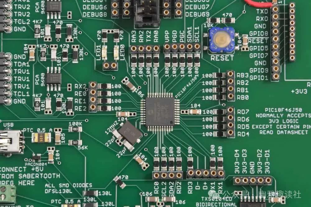
In modern high-frequency microwave circuit design, vertical interconnect transition structures serve as critical paths for signal transmission between different layers of PCBs, and their performance directly affects the overall properties of the system. As communication systems advance into the millimeter-wave frequency band, traditional via structures can no longer meet the integrity requirements for high-frequency signals. The impedance matching, suppression of parasitic effects, and loss control of transition structures have become urgent technical challenges.Electromagnetic Characteristics Analysis of Vertical Interconnect StructuresThe vertical interconnect transition structures mainly include Through Hole Vias, Buried Vias, and Blind Vias. In the microwave frequency band, these structures introduce parasitic inductance and capacitance, leading to impedance discontinuities, signal reflections, and radiation losses. Particularly, when the frequency exceeds 10GHz, the Via Stub Effect can cause resonances that severely degrade signal transmission quality, manifesting as deep dips in the S-parameters.Through equivalent circuit modeling, a typical via can be represented as an LC network composed of inductance L_via, capacitance C_pad, and C_anti-pad. In a 5G system operating at 28GHz, a standard 8mil diameter via may produce approximately 0.2nH of parasitic inductance, which is sufficient to introduce significant phase delay and amplitude attenuation in signal transmission.Optimization Design MethodsFor microwave PCB vertical interconnect structures, the following optimization methods have proven effective:Via Stub Elimination Technique: Using back drilling to remove unnecessary portions of the via can improve the reflection coefficient S11 from -10dB to below -20dB. For higher performance requirements, laser drilling can be considered to form a stepped via structure.Impedance Matching Optimization: By adjusting the via pad size and the solder mask opening size, the values of C_pad and C_anti-pad can be finely controlled. Our tests indicate that in a Coplanar Waveguide with Ground (CPWG) structure, appropriately matching the pad diameter with the line width can keep the impedance variation in the transition region within ±5%.Ground Plane Treatment: Distributing grounding vias around the via to form a complete return path is essential. Measured data shows that in 24GHz applications, when the spacing between grounding vias is less than λ/20, the generation of Parallel Plate Mode can be effectively suppressed.Transition Structure Topology Optimization: For the transition from microstrip to stripline, using a tapered transition structure can reduce insertion loss by more than 0.3dB compared to a direct connection and increase bandwidth by approximately 30%. Simulation and Measurement ValidationIt is essential to validate the optimized design using three-dimensional electromagnetic simulation software (such as HFSS, CST). Notably, the precise setting of material parameters in the model is crucial, especially the loss tangent (tanδ) of dielectric materials at high frequencies should use frequency-dependent models.Our test samples made from Rogers RO4350B material (εr=3.48, tanδ=0.0037@10GHz) show that the optimized vertical interconnect structure maintains a reflection coefficient below -15dB across the DC-40GHz range, with insertion loss less than 0.5dB. Compared to the standard design, the optimized structure improves signal integrity metrics by approximately 60% in the millimeter-wave frequency band.Practical Design GuidelinesBased on theoretical analysis and engineering practice, the following design guidelines are proposed:The ratio of via diameter to dielectric height (d/h) should be controlled within the range of 0.5-0.7.The spacing of grounding vias should not exceed 1/8 of the wavelength at the highest operating frequency.At least 3-4 symmetrically distributed grounding vias should be configured around signal vias.In high-frequency applications, the pad diameter should be kept as small as possible to reduce parasitic capacitance.ConclusionOptimizing vertical interconnect transition structures for microwave circuit boards is an essential aspect of high-frequency PCB design. Through precise electromagnetic analysis and systematic optimization methods, the quality of signal transmission between layers can be significantly enhanced. With the development of technologies such as 5G millimeter waves, radar, and high-speed optical communication, this field will continue to face higher challenges, requiring design engineers to balance theoretical analysis with practical processes to achieve high-performance, low-cost design goals.