How does traditional plating address the “dog bone effect” and void defects when the aspect ratio of the interlayer vias exceeds 10:1?
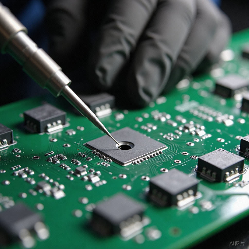
Technical Principles and Process Challenges
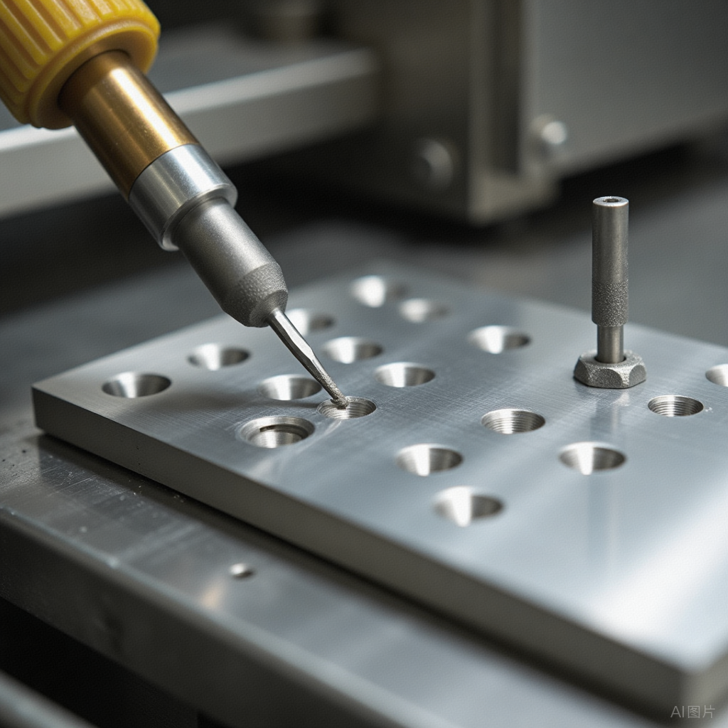
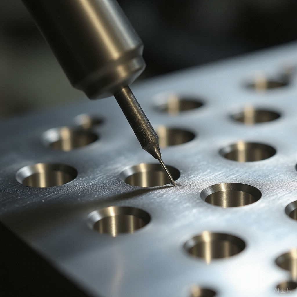
Structural Characteristics of Blind and Buried Vias
- Definition Differences
- Blind Via: Connects outer layers to inner layers, typically 50-200μm deep
- Buried Via: Completely embedded within inner layers, aspect ratios can reach 15:1 (e.g., 0.1mm diameter / 1.5mm depth)
- Plating Challenges Matrix
Issue Physical Cause Consequence Layer buildup at via openings Uneven current density distribution (edge effect) Bridge breakage in solder mask (gap < 25μm) Thin copper in the middle of the via Insufficient ion diffusion rate Impedance fluctuation (±8%) Bottom voids Hydrogen bubble entrapment Thermal cycling failure (cracking after >300 cycles)

Electrochemical Kinetics Model described by the Butler-Volmer equation:
i = i_0 \left[ \exp\left(\frac{\alpha nFη}{RT}\right) - \exp\left(-\frac{(1-\alpha)nFη}{RT}\right) \right]
Where:
- (i_0) Exchange current density: Typical value for acidic copper plating solution is 0.5-2 A/dm²
- (α) Transfer coefficient: 0.3-0.7 (depends on additive system)
Case Validation: A 6-layer HDI board using pulse reverse plating improved the copper thickness uniformity from ±35% to ±8% (measured by SEM cross-section)
Core Process Solutions
Horizontal Pulse Plating System (HPS)
- Three-Stage Current Control
- Forward Pulse (50ms On, 10A/dm²): Initiates deposition at the bottom of deep vias
- Reverse Stripping (5ms Off, -3A/dm²): Dissolves excessively thick copper layers at the via openings
- Relaxation Period (20ms): Promotes ion diffusion (Cu²+ concentration gradient reduced by 62%)
- Titanium basket anode (containing 0.03% phosphorus, uniformity improved by 40%)
- Jet system (3m/s flow rate to flush bubbles from within the vias)
Additive Chemical System
- Functional Component Ratios
Component Concentration Range Mechanism Supplier Example Sodium Polysulfide (SPS) 2-5ppm Accelerator (reduces polarization resistance) Atotech Cupracid Polyethyleneimine (PEI) 50-100ppm Inhibitor (preferentially adsorbs in high current areas) Enthone ViaForm Chloride Ions 40-60ppm Complexing agent (stabilizes Cu⁺ intermediate state) MacDermid MCM
Experimental Data: In blind vias with an aspect ratio of 12:1, the optimal additive combination improved coating ductility from 15% to 28% (ASTM E8 standard test)
Process Monitoring and Defect Prevention
Online Monitoring Technology
- Hall Cell Testing (hourly sampling):
- Monitors decomposition products of additives (e.g., SPS → MPS conversion rate >20% requires replenishment)
- Constant Potential Meter (LPR)
- Real-time measurement of polarization resistance (abnormal fluctuations >5% trigger alarms)
Typical Defect Solutions
- “Volcano” Phenomenon
- Cause: Residual photoresist leads to local insulation
- Countermeasure: Plasma de-gluing (O₂/N₂ mixed gas, 200W RF power)
- Dendritic Crystallization
- Cause: Excess chloride ions (>80ppm)
- Countermeasure: Activated carbon filtration (adsorption capacity ≥0.5g/g)
Industrial Application Cases
Automotive Radar PCB (77GHz)
- Requirements
- 20-layer board, buried via aspect ratio 10:1
- High-frequency loss < 0.02dB/cm @ 76.5GHz
- Solution
- Adopted semi-additive process (mSAP):
- Chemical copper plating (0.3μm seed layer)
- Pattern plating (5μm thick, uniformity ±3%)
- Flash etching to remove excess copper
- Impedance control accuracy ±2Ω (original ±5Ω)
- Production yield increased from 82% to 96%
Server Motherboard (PCIe 5.0)
- Innovations
- Nanowire diameter 80nm, length-to-diameter ratio >1000
- Conductive resistance reduced by 45%
- Copper nanowire filling technology (conductive first, then plating):
Technical Economic Analysis
| Item | Traditional DC Plating | Pulse Filling Plating | Difference |
|---|---|---|---|
| Copper Consumption (kg/m²) | 1.2 | 0.8 | -33% |
| Wastewater Treatment Cost | ¥15/piece | ¥9/piece | -40% |
| Equipment Investment | ¥8 million | ¥12 million | +50% |
| Total Cost (24 months) | ¥2.3 million | ¥1.8 million | -22% |
Interactive Topics:
- When PCB routing density exceeds 10μm line width, should filling plating introduce atomic layer deposition (ALD) as a seed layer?
- In high-frequency signal transmission, how can the effect of copper grain orientation (111) on insertion loss be quantified?
- In vertical stacking packaging (3D IC), what are the essential differences between TSV plating and blind/buried via processes?
- What are the feasibility boundaries of cyanide-free plating solutions in high-speed copper plating?
- Can artificial intelligence achieve zero-defect plating through real-time adjustment of pulse parameters?
Topic Tags:#HighDensityInterconnect #PulsePlating #PCBManufacturing #NanoCopperFilling #ElectrochemicalEngineering

 Chew on this, and we hope our content inspires you. You can also follow our other recommended channels.Capture every little happiness in life, starting today, and let the unknown beauty be within reach. Choose your favorite items and embark on a wonderful journey now!!
 Follow and like for continuous good luck! Clickto see your best!