Understanding PCB Layers: Differences in Solder Paste
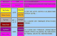
Definition of PCB Layers: Solder mask layer: solder mask, refers to the part of the board where green oil is applied; since it is a negative output, the part with solder mask actually does not have green oil but is plated with tin, appearing silver-white! Paste mask layer: paste mask, is used during machine placement, … Read more