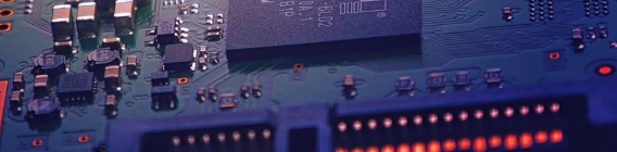
 Vias are one of the essential components of multilayer PCB boards, with drilling costs typically accounting for 30% to 40% of the PCB manufacturing costs. Simply put, every hole on a PCB can be referred to as a via. Functionally, vias can be divided into two categories:
- One is used for electrical connections between layers.
- The other is used for fixing or positioning components.
From a manufacturing process perspective, these vias are generally classified into three types: blind vias, buried vias, and through vias.Blind Vias These are located on the top and bottom surfaces of the printed circuit board and have a certain depth, used for connecting surface traces to inner layer traces. The depth of the hole usually does not exceed a certain ratio (hole diameter).Buried Vias These refer to connection holes located within the inner layers of the printed circuit board, which do not extend to the surface of the board.Both types of vias are located within the inner layers of the board and are formed using through-hole technology before lamination. During the via formation process, several inner layers may overlap.Through Vias These holes pass through the entire PCB and can be used for internal interconnections or as mounting holes for components. Due to the easier manufacturing process and lower cost, most printed circuit boards use through vias rather than the other two types. Unless otherwise specified, the vias discussed here are considered through vias. From a design perspective, a via mainly consists of two parts:one is the drill hole, and the other is the pad area surrounding the drill hole.The sizes of these two parts determine the size of the via. Clearly, in high-speed, high-density PCB designs, the smaller the via, the better, as this allows for more routing space on the board. Additionally, smaller vias have lower parasitic capacitance, making them more suitable for high-speed circuits. However, reducing the hole size also increases costs, and the size of the vias cannot be reduced indefinitely due to limitations in drilling and plating technologies:The smaller the hole, the longer it takes to drill, and the more likely it is to deviate from the center position;and when the depth of the hole exceeds six times the diameter of the drill, it becomes impossible to ensure uniform copper plating on the hole walls. For example, if a standard 6-layer PCB has a thickness (via depth) of 50 mils, the drill diameter that PCB manufacturers can typically provide is only 8 mils under normal conditions. With the development of laser drilling technology, the size of drill holes can become smaller, and vias with a diameter of 6 mils or less are referred to as microvias.Microvias are often used in HDI (High-Density Interconnect) designs, allowing vias to be directly placed on pads (Via-in-pad), significantly improving circuit performance and saving routing space. Vias manifest as points of impedance discontinuity on transmission lines, which can cause signal reflections.The equivalent impedance of a typical via is about 12% lower than that of the transmission line; for example, a 50-ohm transmission line will see its impedance drop by 6 ohms when passing through a via (the exact amount depends on the size of the via and the board thickness). However, the reflections caused by the impedance discontinuity of vias are minimal, with a reflection coefficient of:(44-50)/(44+50)=0.06 The issues caused by vias are more concentrated on the effects of parasitic capacitance and inductance.Parasitic Capacitance of Vias Vias inherently possess parasitic capacitance to ground. If the diameter of the isolation hole on the ground layer is D2, the diameter of the via pad is D1, the thickness of the PCB is T, and the dielectric constant of the substrate is ε, the parasitic capacitance of the via can be approximated as:C=1.41εTD1/(D2-D1) The main effect of the parasitic capacitance of vias on the circuit is to prolong the signal rise time, thereby reducing the circuit speed. For example, for a PCB with a thickness of 50 mils, if a via with an inner diameter of 10 mils and a pad diameter of 20 mils is used, and the distance from the pad to the ground copper area is 32 mils, we can use the above formula to approximate the parasitic capacitance of the via as:C=1.41×4.4×0.050×0.020/(0.032-0.020)=0.517pF The change in rise time caused by this capacitance is:T10-90=2.2C(Z0/2)=2.2×0.517x(55/2)=31.28ps From these values, it can be seen that although the effect of the parasitic capacitance of a single via on rise time is not very significant, designers should still consider it carefully when multiple vias are used for inter-layer switching.Parasitic Inductance of Vias Similarly, vias also have parasitic inductance in addition to parasitic capacitance. In high-speed digital circuit design, the impact of parasitic inductance from vias often outweighs that of parasitic capacitance.Its parasitic series inductance can weaken the contribution of bypass capacitors, reducing the filtering effectiveness of the entire power system. We can use the following formula to roughly calculate the parasitic inductance of a via:L=5.08h[ln(4h/d)+1] Where L is the inductance of the via, h is the length of the via, and d is the diameter of the center drill.From this formula, it can be seen that the diameter of the via has a smaller effect on inductance, while the length of the via has a more significant impact. Using the previous example, we can calculate the inductance of the via as:L=5.08×0.050[ln(4×0.050/0.010)+1]=1.015nH If the signal rise time is 1ns, then its equivalent impedance is:XL=πL/T10-90=3.19Ω This level of impedance cannot be ignored when high-frequency currents are present, especially since bypass capacitors need to connect through two vias when linking power and ground layers, which can significantly increase the parasitic inductance of the vias.Via Design in High-Speed PCBs Through the analysis of the parasitic characteristics of vias, we can see that in high-speed PCB design, seemingly simple vias can often bring significant negative effects to circuit design. To minimize the adverse effects of parasitic effects from vias, designers can aim to achieve the following:
- From both cost and signal quality perspectives, choose vias of reasonable sizes. For example, for PCB designs of 6-10 layer memory modules, using vias of 10/20 mils (drill/pad) is preferable. For some high-density, small-sized boards, 8/18 mil vias can also be considered.Currently, it is challenging to use smaller vias.For power or ground vias, larger sizes can be considered to reduce impedance.
- The two formulas discussed above indicate that using thinner PCBs is beneficial for reducing the two parasitic parameters of vias.
- Power and ground pins should have vias placed nearby, and the leads between the vias and pins should be as short as possible, as longer leads can increase inductance. Additionally, power and ground leads should be as thick as possible to reduce impedance.
- Signal traces on the PCB should avoid layer changes whenever possible, thus minimizing unnecessary vias.
- Place some ground vias near the vias used for signal layer changes to provide a nearby return path for the signal. It may even be beneficial to place several extra ground vias on the PCB. Of course, flexibility in design is also necessary.The via model discussed earlier assumes that each layer has pads; sometimes, we can reduce or even eliminate pads on certain layers.
Especially in cases of very high via density, it may lead to the formation of a break in the copper layer, creating a disconnected loop. To solve this issue, in addition to moving the via positions, we can also consider reducing the pad size of the vias in that copper layer. How to use vias:Through the analysis of the parasitic characteristics of vias, we can see that in high-speed PCB design, seemingly simple vias can often have significant negative effects on circuit design when used improperly.