Hidden Circuit Board Tunnels – Buried Vias
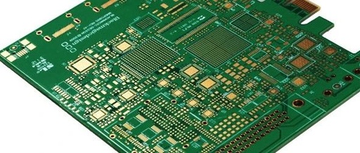
Hidden Circuit Board Tunnels - Buried Vias

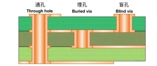
1.Definition A PCB buried via is a hole that connects different layers of conductive traces within a multilayer printed circuit board. Unlike through holes and blind vias, buried vias are completely hidden inside the PCB and are not visible on the surface. This design allows the PCB to maintain high-density routing while optimizing signal transmission … Read more

Critical Blind and Buried Via Technology in PCB Design

Critical Blind and Buried Via Technology in PCB Design

Recently, I encountered a customer complaint regarding PCBA blind and buried via issues. I took this opportunity to study the topic and share knowledge with my colleagues and friends. **Core Concept:** In traditional PCB design, vias (referred to as “through holes” or “vias”) that connect different layers of circuits are through holes that extend from … Read more

Blind and Buried Via Plating Technology: Decoding the Precision Process of High-Density Interconnect PCB Manufacturing

Blind and Buried Via Plating Technology: Decoding the Precision Process of High-Density Interconnect PCB Manufacturing

How does traditional plating address the “dog bone effect” and void defects when the aspect ratio of the interlayer vias exceeds 10:1? Technical Principles and Process Challenges Structural Characteristics of Blind and Buried Vias Definition Differences Blind Via: Connects outer layers to inner layers, typically 50-200μm deep Buried Via: Completely embedded within inner layers, aspect … Read more

The Impact of PCB Vias on Heat Dissipation

The Impact of PCB Vias on Heat Dissipation

In natural convection heat dissipation products, the size of vias on the PCB has a significant impact on heat dissipation. However, the exact extent of this impact is still unknown. We will start with a simple product analysis, focusing on the via parameters of a single chip, to study how changes in via parameters affect … Read more