Today, we will share technical knowledge about vias and back drilling in PCBs.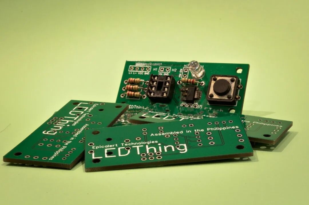
1. Via Design in High-Speed PCBs
In high-speed PCB design, multi-layer PCBs are often required, and vias are an important factor in multi-layer PCB design.
The vias in a PCB mainly consist of three parts: the hole, the pad area around the hole, and the POWER layer isolation area.
1. Impact of Vias in High-Speed PCBs
In multi-layer high-speed PCBs, signals need to pass through vias to connect from one layer of interconnect to another. At frequencies below 1 GHz, vias can provide good connectivity, and their parasitic capacitance and inductance can be ignored.
However, when the frequency exceeds 1 GHz, the parasitic effects of vias cannot be ignored, as they behave as points of impedance discontinuity in the transmission path, leading to signal integrity issues such as reflection, delay, and attenuation.
When a signal is transmitted through a via to another layer, the reference layer of the signal line also serves as the return path for the via signal, and the return current flows through capacitive coupling between reference layers, causing issues like ground bounce.
2. Types of Vias
Vias are generally divided into three categories: through holes, blind holes, and buried holes.
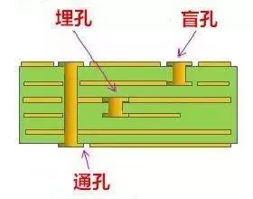
Blind Holes:These are located on the top and bottom surfaces of the printed circuit board, with a certain depth, used to connect surface lines to inner layer lines. The depth of the hole does not exceed a certain ratio compared to the hole diameter.
Buried Holes:These are connection holes located within the inner layers of the printed circuit board and do not extend to the surface of the board.
Through Holes:This type of hole passes through the entire circuit board and can be used for internal interconnections or as mounting holes for components. Through holes are generally easier to implement in manufacturing and are lower in cost, so they are commonly used in printed circuit boards.
3. Via Design in High-Speed PCBs
In high-speed PCB design, seemingly simple vias can often have significant negative effects on circuit design. To minimize the adverse effects of parasitic effects from vias, the following design considerations can be made:
(1) Choose appropriate via sizes. For multi-layer PCBs of general density, vias of 0.25mm/0.51mm/0.91mm (drill/pad/POWER isolation area) are preferable; for high-density PCBs, vias of 0.20mm/0.46mm/0.86mm can also be used, and non-through vias can be considered; for power or ground vias, larger sizes can be used to reduce impedance;
(2) The POWER isolation area should be as large as possible, considering the via density on the PCB, generally D1=D2+0.41;
(3) Signal traces on the PCB should avoid layer changes as much as possible, meaning reducing the number of vias;
(4) Using thinner PCBs helps reduce the two parasitic parameters of vias;
(5) Power and ground pins should be close to vias, and the lead between the via and the pin should be as short as possible, as they can increase inductance. Additionally, power and ground leads should be as thick as possible to reduce impedance;
(6) Place some ground vias near signal layer change vias to provide a short return path for the signal.
Moreover, the length of the via is also one of the main factors affecting via inductance. For vias used for top and bottom layer conduction, the via length equals the PCB thickness. As the number of PCB layers increases, the PCB thickness often exceeds 5 mm. However, in high-speed PCB design, to minimize issues caused by vias, the via length is generally controlled to be within 2.0 mm. For vias longer than 2.0 mm, increasing the via diameter can improve via impedance continuity to some extent. When the via length is 1.0 mm or less, the optimal via diameter is 0.20 mm to 0.30 mm.
2. Back Drilling Process in PCB Production
1. What is PCB Back Drilling?
Back drilling is a special type of deep drilling. In the production of multi-layer boards, for example, when making a 12-layer board, we need to connect layer 1 to layer 9. Typically, we drill a through hole (first drilling) and then plate copper. This connects layer 1 directly to layer 12, but we only need layer 1 to connect to layer 9. Layers 10 to 12 do not have any connections and act like a column.
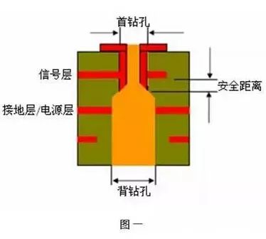
This column affects the signal path and can cause signal integrity issues in communication signals. Therefore, this unnecessary column (referred to as a STUB in the industry) is drilled out from the back (second drilling). Hence, it is called back drilling, but it is generally not drilled completely clean, as subsequent processes will electrolyze away some copper, and the drill tip itself is also sharp. Therefore, PCB manufacturers will leave a small amount, and the remaining length of the STUB is called the B value, which is generally best kept in the range of 50-150UM.
2. What are the advantages of back drilling?
1) Reduces noise interference;
2) Improves signal integrity;
3) Reduces local board thickness;
4) Reduces the use of buried and blind holes, lowering PCB manufacturing difficulty.
3. What is the function of back drilling?
The function of back drilling is to remove the segments of through holes that do not serve any connection or transmission purpose, avoiding reflections, scattering, delays, and distortion in high-speed signal transmission. Research shows that the main factors affecting signal integrity in signal systems, aside from design, board materials, transmission lines, connectors, and chip packaging, include through holes, which have a significant impact on signal integrity.
4. What is the working principle of back drilling production?
It relies on the microcurrent generated when the drill tip contacts the copper foil on the surface of the substrate to sense the height of the board surface, and then drills down to the set depth. Drilling stops when the set depth is reached. As shown in Figure 2:
5. What is the process flow for back drilling production?
a. Provide the PCB, which has positioning holes, and use these positioning holes to perform initial drilling and drilling;
b. Electroplate the PCB after the first drilling, and perform dry film sealing on the positioning holes before electroplating;
c. Create outer layer patterns on the electroplated PCB;
d. Perform pattern electroplating on the PCB after forming the outer layer pattern, and perform dry film sealing on the positioning holes before pattern electroplating;
e. Use the positioning holes from the first drilling for back drilling positioning, and use a drill to back drill the electroplated holes that need back drilling;
f. After back drilling, wash the back drilled holes to remove any remaining drill chips.
6. What are the technical features of back drilled boards?
1) Most back plates are rigid boards;
2) The number of layers is generally between 8 and 50 layers;
3) Board thickness: over 2.5mm;
4) High aspect ratio;
5) Larger board dimensions;
6) The minimum hole diameter for the first drill is generally >=0.3mm;
7) Fewer outer layer traces, mostly designed as arrays of press-fit holes;
8) Back drilled holes are usually 0.2MM larger than the holes that need to be drilled out;
9) Back drilling depth tolerance: +/-0.05MM;
10) If back drilling is required to reach layer M, then the minimum dielectric thickness from layer M to layer M-1 (the layer below M) must be 0.17MM;
7. In which fields are back drilled boards mainly applied?
Back plates are mainly used in communication equipment, large servers, medical electronics, military, aerospace, and other fields.
Copyright statement: The copyright of this article belongs to the original author and does not represent the views of this account. The articles pushed by this account are for sharing purposes only and do not represent the position of this account. If there are any copyright issues, please contact us for deletion.