PCBEngineers often find multilayer circuit boards confusing at first glance, especially with layers reaching ten or more, resembling a spider web.Below are several internal structure diagrams of multilayer PCBs, showcasing various stacking structures in a three-dimensional format.
01
The core of High-Density Interconnect (HDI) boards lies in the vias.
The processing of multilayer PCB traces is not much different from that of single or double-layer boards; the main difference lies in the via technology.
Traces are etched, while vias are drilled and then plated with copper, which is well understood by those involved in hardware development, so I won’t elaborate further.
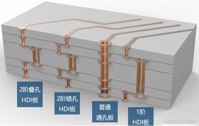
Multilayer circuit boards typically include through-hole boards, first-order boards, second-order boards, and second-order stacked via boards. Higher-order boards, such as third-order boards and arbitrary layer interconnect boards, are rarely used and are extremely expensive, so I won’t discuss them in detail.
Generally, 8-bit microcontroller products use 2-layer through-hole boards; smart hardware at the 32-bit microcontroller level uses 4 to 6-layer through-hole boards; Linux and Android-level smart hardware uses 6 to 8-layer first-order HDI boards; compact products like smartphones typically use 8-layer first-order to 10-layer second-order circuit boards.
8-layer second-order stacked vias, Qualcomm Snapdragon 624
02
The most common through-hole.
There is only one type of via that connects from the first layer to the last layer. Regardless of whether the traces are external or internal, the holes are drilled through, known as through-hole boards.
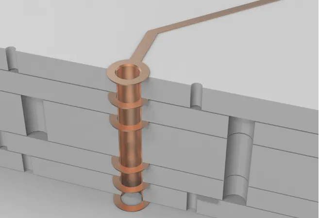
Through-hole boards are not related to the number of layers; commonly used 2-layer boards are through-hole boards, while many switches and military circuit boards can have 20 layers and still be through-hole.Using a drill to penetrate the circuit board and then plating copper in the holes forms the pathways.It is important to note that the inner diameters of through-holes are usually 0.2mm, 0.25mm, and 0.3mm, but generally, 0.2mm is significantly more expensive than 0.3mm. This is because thinner drill bits are more prone to breaking and take longer to drill. The additional time and cost of drill bits are reflected in the increased price of the circuit board.03
Laser vias in High-Density Boards (HDI boards).
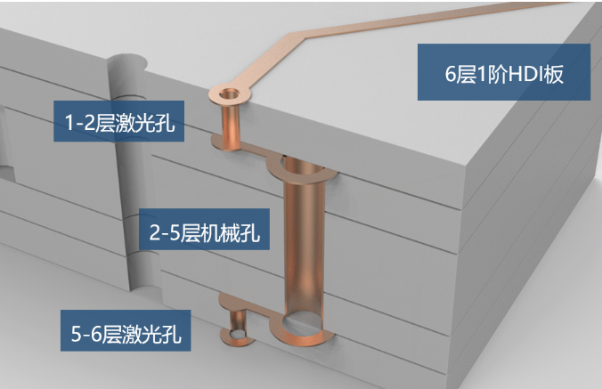
This image shows the stacking structure of a 6-layer first-order HDI board, where the top two layers are laser vias with a 0.1mm inner diameter. The inner layers are mechanical vias, equivalent to a 4-layer through-hole board, covered by two additional layers.
Lasers can only penetrate fiberglass materials, not metal copper. Therefore, drilling holes on the outer surface does not affect other internal traces.
After the laser creates the holes, copper is plated to form laser vias.
04
Second-order HDI board with two layers of laser vias.
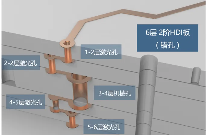
This image depicts a 6-layer second-order staggered via HDI board. Typically, 6-layer second-order boards are less common, with most starting from 8 layers. The additional layers follow the same principle as the 6-layer boards.
The term second-order refers to having two layers of laser vias.
The term staggered vias means that the two layers of laser vias are offset.
Why offset? Because copper plating cannot fill the vias completely, leaving them hollow inside, so additional holes cannot be drilled directly on top; they must be offset by a certain distance before drilling another layer of holes.
6-layer second-order = 4-layer first-order plus 2 additional layers.
8-layer second-order = 6-layer first-order plus 2 additional layers.
05
Stacked via boards have more complex processes and higher prices.
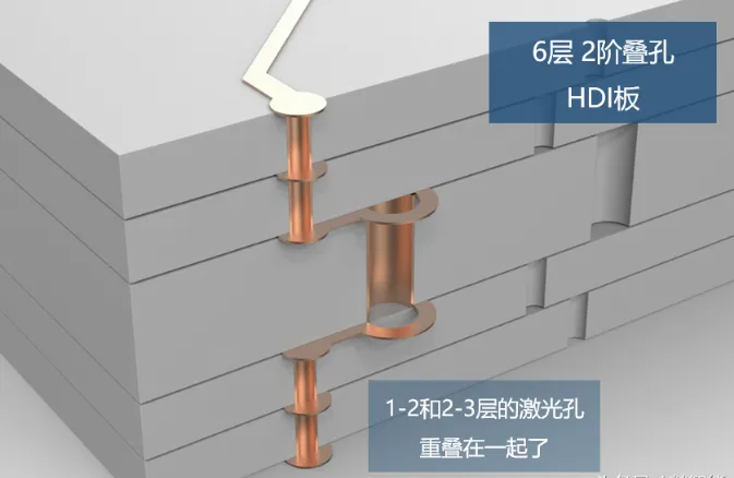
In staggered via boards, the two layers of laser vias overlap. This results in a more compact layout.
It is necessary to electroplate the inner laser vias to fill them before creating the outer laser vias. This process is slightly more expensive than staggered vias.
06
Extremely expensive arbitrary layer interconnect boards with multiple laser stacked vias.
Each layer consists of laser vias, allowing for flexible routing and hole placement.
Layout engineers must find this exhilarating! No longer fearing that they can’t design the layout!
Procurement teams might find this distressing, as it costs over ten times more than standard through-hole boards!
Thus, only products like the iPhone can afford to use them. Other smartphone brands have not been reported to use arbitrary layer interconnect boards.
Conclusion
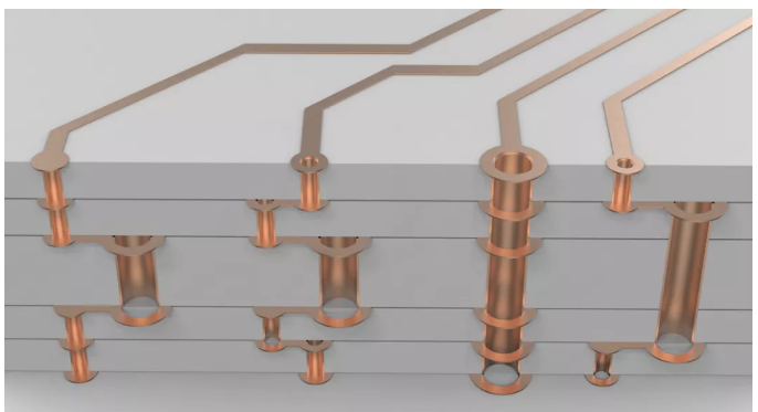
Finally, here is an image for a detailed comparison.
Please pay attention to the size of the holes and whether the pads are closed or open.
Statement:The copyright of this article belongs to the original author and does not represent the views of the association.The articles shared by the “Jiangxi Province Electronic Circuit Industry Association” are for sharing purposes only and do not represent the position of this account. If there are any copyright issues, please contact us for removal.