Recently, I encountered a customer complaint regarding PCBA blind and buried via issues. I took this opportunity to study the topic and share knowledge with my colleagues and friends.
**Core Concept:** In traditional PCB design, vias (referred to as “through holes” or “vias”) that connect different layers of circuits are through holes that extend from the top layer to the bottom layer. However, as electronic products evolve towards miniaturization, lightweight design, and high performance, the density of components on PCBs is increasing, and routing space is becoming tighter. Traditional through holes occupy a significant amount of space, limiting routing density and design flexibility. The blind and buried via technology has been developed as a core component of high-density interconnect technology to address this issue. It includes two main types of non-through vias:
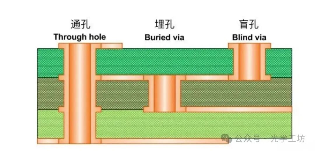
1. Blind Via: Definition: A via that starts from the outer layer of the PCB (top or bottom layer) and terminates at an inner layer, but does not go through the entire thickness of the board. Characteristics: It can only be seen from one surface of the board. It connects the outer layer to one or more inner layers. The depth is less than the board thickness. Function: It frees up valuable routing space on the outer layer, allowing for more components or traces to be placed on the outer layer. 2. Buried Via: Definition: A via that is completely located between the internal layers of the PCB, connecting neither the top layer nor the bottom layer. Characteristics: It cannot be seen from either of the two outer surfaces of the PCB. It only connects inner layers (e.g., L2-L3, L3-L4, etc.). It is completely enclosed within the multilayer board. Function: It frees up space on all outer and inner layers, greatly enhancing the freedom and density of inner layer routing, making it the highest-level density enhancement technology. Why is blind and buried via technology necessary? 1. Increase Routing Density: This is the primary reason. Through holes occupy space across all layers of the board. Blind vias occupy only part of the layers, while buried vias do not occupy any outer layer space, freeing up more valuable surface and internal space for routing. 2. Reduce PCB Size: Higher routing density means that the same functionality can be achieved on a smaller board, or more complex functions can be realized on a small-sized board. This is crucial for smartphones, wearable devices, and high-end digital products. 3. Enhance Signal Integrity: Shorten Signal Paths: Blind and buried vias can connect the layers that need interconnection more directly, significantly reducing the distance of signal transmission (especially for high-speed signals), thereby reducing signal delay and transmission line effects. Reduce Via Stubs: Through holes leave unconnected “stubs” on layers where connections are not needed. These stubs act like antennas, reflecting signals and causing ringing and signal distortion. Blind and buried vias exist only in the layers that need to be connected, resulting in almost no stubs, significantly improving the integrity of high-speed signals (reducing reflections and crosstalk). 4. Optimize Power/Ground Planes: Using buried vias to connect inner layer power and ground planes can reduce the cutting of complete power/ground planes by through holes, maintaining the integrity of the planes and providing better power integrity and electromagnetic compatibility. 5. Support Smaller Pitch BGA Chips: Modern high-density BGA chips (such as CPUs, GPUs, and FPGAs) have very small pin pitches (<0.8mm). Using blind and buried vias in the area beneath their pads is the only feasible routing solution, as through holes cannot effectively fan out traces in such a small area. 6. Achieve More Complex Multilayer Board Designs: For complex PCBs with 12 layers, 16 layers, or even more, blind and buried via technology is essential for achieving flexible and efficient interconnections between layers.
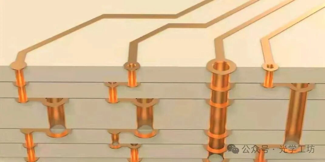
Manufacturing Process of Blind and Buried Via Technology (Key Challenges): Manufacturing blind and buried vias is much more complex than manufacturing through holes, and the costs are significantly higher. The main challenges lie in multiple lamination and precision drilling/laser drilling. 1. Layered Manufacturing: The PCB is no longer simply stacked with all layers and drilled at once. It requires phased manufacturing: Inner layer core board production: First, produce the inner layer core boards that include buried vias (if needed) (e.g., L2-L3). These core boards undergo drilling, copper plating, etching, and other processes before lamination. First Lamination: Laminate the produced inner layer core boards with prepreg. Laser Drilling: Use high-precision lasers (such as CO2 lasers or UV lasers) to drill blind vias in the laminated multilayer board (connecting outer and inner layers). Lasers can precisely control the depth of the holes. Blind Via Metallization: Metallize the drilled blind vias (copper deposition, electroplating) to form conductive pathways. Outer Layer Pattern Transfer and Etching: Create the outer layer circuit patterns. Possible Phased Repetition: For more complex boards (such as those requiring different depths of blind vias or step vias), multiple laminations, laser drilling, via metallization, and pattern transfer cycles may be necessary. 2. Precision Alignment: The multiple lamination and processing steps require extremely high alignment accuracy between layers (usually in the tens of micrometers). Misalignment can cause blind and buried vias to be misaligned with target pads, leading to open circuits or reliability issues. 3. Material Selection: The multiple lamination process imposes higher requirements on the performance of substrate materials and prepregs (such as thermal resistance and dimensional stability). 4. Cost and Lead Time: The complex process, expensive laser drilling equipment, high yield requirements, and longer production cycles make the cost of PCBs using blind and buried via technology significantly higher than that of ordinary through-hole boards, and the production lead time is also longer. Application Scenarios: Blind and buried via technology is widely used in electronic products that require high density, high performance, and miniaturization: 1. Smartphones and tablets 2. Laptops and ultrabooks 3. Wearable devices (smartwatches, headphones) 4. High-end digital cameras 5. Network communication devices (routers, switches, base stations) 6. Servers and data center hardware 7. Aerospace and defense electronics 8. High-end medical devices 9. Automotive electronics (ADAS, infotainment systems) Conclusion: The blind and buried via technology in PCBA (including blind vias and buried vias) is the cornerstone of modern high-density interconnect PCB design. It greatly saves routing space, increases routing density, reduces board size, and significantly enhances the integrity of high-speed signals through non-through hole connections. Despite its complex manufacturing process and high costs, it is an indispensable key technology in the pursuit of miniaturization and high performance in electronic devices. As electronic products continue to evolve towards smaller, faster, and smarter designs, the application of blind and buried via technology will become increasingly common and profound.