#XCVU9P-2FLGC2104I #Xilinx #AMD #VirtexUltraScale+ FPGA is a flagship model designed for high-performance logic, #data center interconnect, #industrial signal processing, 5G front-haul and core networks, #ultra-high bandwidth image processing, and #algorithm acceleration. This device is built on a 16nm FinFET+ process, featuring extremely high logic resource density, a rich set of high-speed transceivers, a wide internal interconnect architecture, scalable DSP computational capabilities, and a highly reliable clock and configuration system.
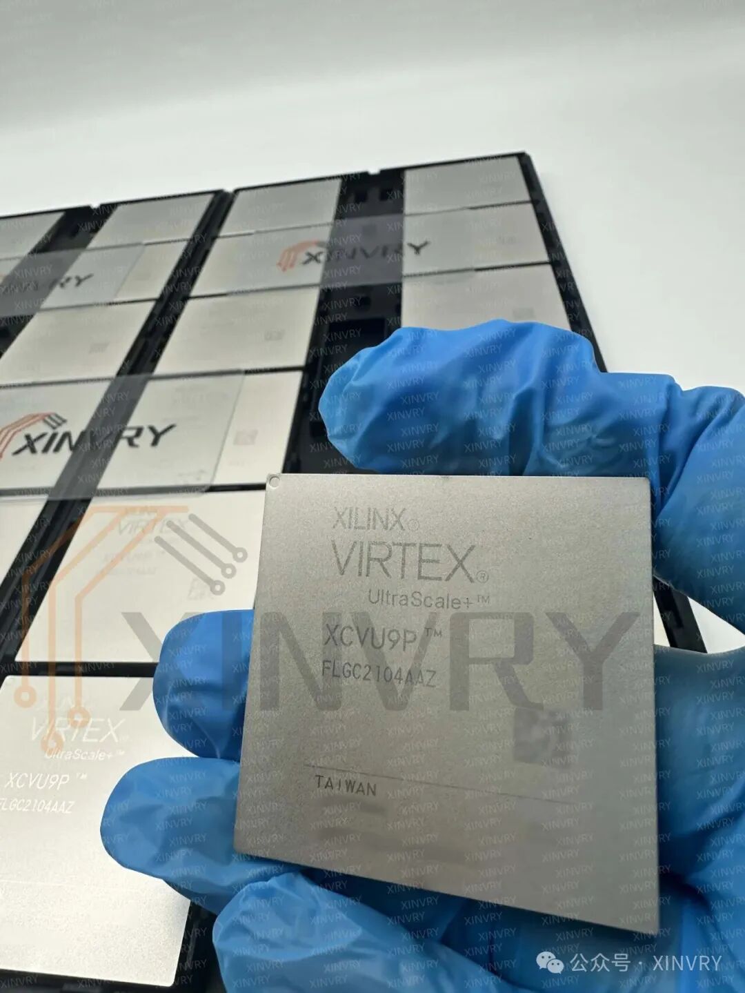
The core of this chip consists of a large number of programmable logic resources and a broadband switching structure. The device includes a massive amount of lookup table logic, distributed registers, ultra-high-speed routing, and predictable timing structures, enabling it to maintain stable compilation times and convergence capabilities in complex state machines, large-scale pipelines, algorithm networks, and multi-module parallel scheduling. A large amount of BRAM and UltraRAM is distributed across the logic array, providing a multi-level storage structure from on-chip caches, deep FIFOs to image buffers and high-speed temporary data access.
This chip is equipped with multiple high-speed GTY or GTH transceivers, with single-channel rates reaching 25Gbps, and supports PCIe, 100G/40G/25G/10G Ethernet, CPRI, JESD204B/C, Aurora, and custom high-speed protocols. These transceivers work in conjunction with the chip’s internal high-speed interconnect structure, allowing for the construction of multiple 100G network ports, optical transmission links, data center accelerator cards, or high-speed backplane switching modules. This is ideal for systems requiring high-throughput networks such as edge computing, data center smart NICs, coprocessors, and FPGA accelerator cards.
The device employs a mature UltraScale+ clock network, including global clocks, multi-region clocks, distributed buffering trees, as well as MMCM and PLL resources, ensuring stable synchronization across different logic regions, SerDes areas, and multiple clock domains. The internal high-speed interconnect is based on an enhanced bidirectional programmable switching structure, significantly reducing inter-region routing delays and improving timing convergence for large-scale designs.
Unlike the Zynq series SoC architecture, the XCVU9P does not include an ARM processor but is a pure FPGA structure. However, its internal resources are sufficient to implement control-type processors through soft cores or to connect to external CPUs/GPUs via PCIe to form heterogeneous acceleration systems. Its high-bandwidth off-chip interfaces support DDR4 multi-channel controllers, enabling the construction of tens of GB/s external memory bandwidth to meet the hardware requirements for video buffering, data packet caching, and temporary storage for deep algorithms.
Xilinx AMD Virtex UltraScale+ FPGA Selection:
XCVU13P-1FHGA2104E, XCVU5P-1FLVA2104EXCVU13P-1FHGA2104I, XCVU5P-1FLVA2104IXCVU13P-1FHGB2104E, XCVU5P-1FLVB2104EXCVU13P-1FHGB2104I, XCVU5P-1FLVB2104IXCVU13P-1FLGA2577E, XCVU5P-1FLVC2104EXCVU13P-1FLGA2577I, XCVU5P-2FLVA2104EXCVU13P-1FSGA2577E, XCVU5P-2FLVA2104IXCVU13P-1FSGA2577I, XCVU5P-2FLVB2104EXCVU13P-2FHGA2104E, XCVU5P-2FLVB2104IXCVU13P-2FHGA2104I, XCVU5P-2FLVC2104EXCVU13P-2FHGB2104E, XCVU5P-3FLVA2104EXCVU13P-2FHGB2104I, XCVU5P-3FLVB2104EXCVU13P-2FHGC2104E, XCVU5P-3FLVC2104EXCVU13P-2FIGD2104E, XCVU5P-L2FLVA2104EXCVU13P-2FIGD2104I, XCVU5P-L2FLVB2104EXCVU13P-2FLGA2577E, XCVU5P-L2FLVC2104EXCVU13P-2FLGA2577I, XCVU7P-1FLVA2104IXCVU13P-2FSGA2577E, XCVU7P-1FLVB2104EXCVU13P-2FSGA2577I, XCVU7P-1FLVB2104IXCVU13P-3FHGA2104E, XCVU7P-2FLVA2104EXCVU13P-3FHGB2104E, XCVU7P-2FLVA2104IXCVU13P-3FHGC2104E, XCVU7P-2FLVB2104EXCVU13P-3FIGD2104E, XCVU7P-2FLVB2104IXCVU13P-3FLGA2577E, XCVU7P-2FLVC2104EXCVU13P-3FSGA2577E, XCVU7P-2FLVC2104IXCVU13P-L2FHGA2104E, XCVU7P-3FLVA2104EXCVU13P-L2FHGB2104E, XCVU7P-3FLVB2104EXCVU13P-L2FHGC2104E, XCVU7P-3FLVC2104EXCVU13P-L2FIGD2104E, XCVU7P-L2FLVA2104EXCVU13P-L2FLGA2577E, XCVU7P-L2FLVB2104EXCVU13P-L2FSGA2577E, XCVU7P-L2FLVC2104E
XCVU19P-2FSVA3824E, XCVU9P-1FLGA2104EXCVU27P-1FIGD2104E, XCVU9P-1FLGA2104IXCVU27P-1FIGD2104I, XCVU9P-1FLGA2577EXCVU27P-1FSGA2577E, XCVU9P-1FLGA2577IXCVU27P-1FSGA2577I, XCVU9P-1FLGB2104EXCVU27P-2FIGD2104E, XCVU9P-1FLGB2104IXCVU27P-2FIGD2104I, XCVU9P-1FLGC2104EXCVU27P-2FSGA2577E, XCVU9P-2FLGA2104EXCVU27P-2FSGA2577I, XCVU9P-2FLGA2104IXCVU27P-L2FIGD2104E, XCVU9P-2FLGA2577EXCVU27P-L2FSGA2577E, XCVU9P-2FLGA2577IXCVU29P-1FIGD2104E, XCVU9P-2FLGB2104EXCVU29P-1FIGD2104I, XCVU9P-2FLGB2104IXCVU29P-1FSGA2577E, XCVU9P-2FLGC2104EXCVU29P-1FSGA2577I, XCVU9P-2FLGC2104IXCVU29P-2FIGD2104E, XCVU9P-2FSGD2104EXCVU29P-2FIGD2104I, XCVU9P-2FSGD2104IXCVU29P-2FSGA2577E, XCVU9P-3FLGA2104EXCVU29P-2FSGA2577I, XCVU9P-3FLGA2577EXCVU29P-L2FIGD2104E, XCVU9P-3FLGB2104EXCVU29P-L2FSGA2577E, XCVU9P-3FLGC2104EXCVU31P-1FSVH1924E, XCVU9P-3FSGD2104EXCVU31P-2FSVH1924E, XCVU9P-L2FLGA2104EXCVU31P-3FSVH1924E, XCVU9P-L2FLGA2577EXCVU31P-L2FSVH1924E, XCVU9P-L2FLGB2104E
XCVU33P-1FSVH2104E, XCVU9P-L2FLGC2104EXCVU33P-2FSVH2104E, XCVU9P-L2FSGD2104EXCVU33P-3FSVH2104E, XCVU11P-1FLGB2104IXCVU33P-L2FSVH2104E, XCVU3P-1FFVC1517EXCVU35P-1FSVH2104E, XCVU3P-2FFVC1517EXCVU35P-1FSVH2892E, XCVU3P-2FFVC1517IXCVU35P-2FSVH2104E, XCVU3P-3FFVC1517EXCVU35P-2FSVH2892E, XCVU3P-L2FFVC1517EXCVU35P-3FSVH2104E, XCVU45P-1FSVH2104EXCVU35P-3FSVH2892E, XCVU45P-1FSVH2892EXCVU35P-L2FSVH2104E, XCVU45P-2FSVH2104EXCVU35P-L2FSVH2892E, XCVU45P-2FSVH2892EXCVU37P-1FSVH2892E, XCVU45P-3FSVH2104EXCVU37P-2FSVH2892E, XCVU45P-3FSVH2892EXCVU37P-3FSVH2892E, XCVU45P-L2FSVH2104EXCVU37P-L2FSVH2892E, XCVU45P-L2FSVH2892EXCVU47P-1FSVH2892E, XCVU47P-3FSVH2892EXCVU47P-2FSVH2892E, XCVU47P-L2FSVH2892EXCVU19P-2FSVB3824E
#XilinxDevelopment #FPGADevelopment #FPGAEngineer