XCVU7P-2FLVB2104E #Xilinx #AMD’s #VirtexUltraScale+ #FPGA (UltraScale+ based on 16nm FinFET+ technology). The #Virtex UltraScale+ is designed for systems requiring extremely high bandwidth, massive parallel computing, and low-latency interconnects: data center acceleration, 400G/800G networks, 5G baseband/remote units, #ASIC prototyping/hardware emulation, and other scenarios.
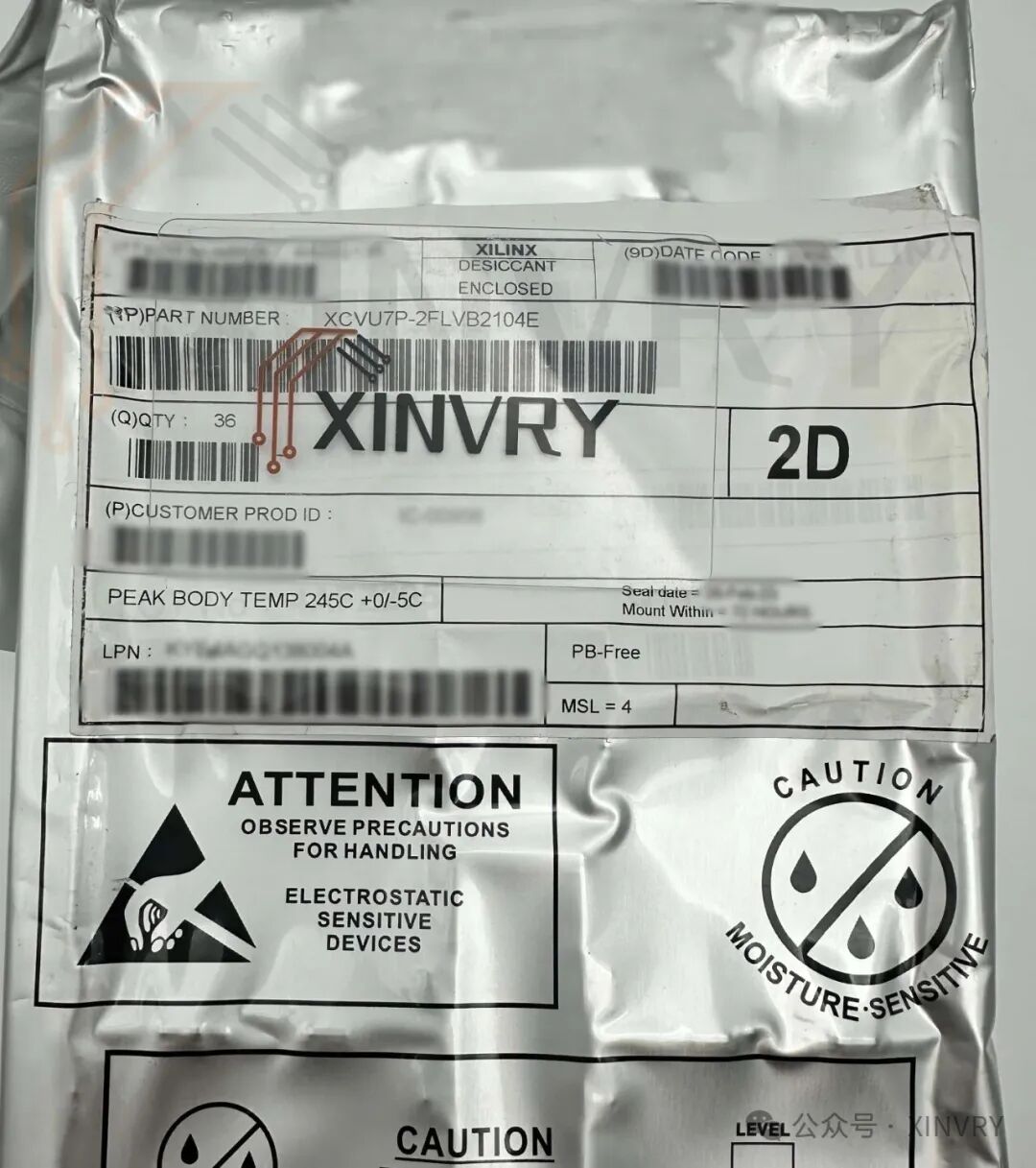
The system logic capacity of XCVU7P is approximately 1.72M system #logic units (about 1,724,100 logic cells), with ALM/CLB granularity at ~98,520 ALM (Adaptive Logic Modules); the hardware DSP slices are around 4,560 slices, and the on-chip memory varies by device variant, providing hundreds of megabits of available on-chip/in-package storage for building deep caches and pipelines. The XCVU7P also integrates a large number of high-speed serial transceivers (typically 80 transceivers, supporting rates up to 32.75 Gb/s), and supports a rich set of on-chip clock/PLL/MMCM resources and hierarchical interconnects to ensure timing closure for complex designs.
“FLVB2104E” indicates the use of a high-pin FCBGA/FLVB 2104 pin package (2104-ball FCBGA), which determines the number of available user I/Os and power routing distribution. The distribution/device page lists the common available I/Os for this package variant at around ~700, with the typical core supply voltage for the device in the range of ~0.825V–0.876V.
The UltraScale+ architecture emphasizes a strategy of “hierarchical storage + hard-core #DSP + low-latency interconnect”: the device internally features distributed LUT-RAM, multiple sets of 18k/36k Block RAM (BRAM/EBR), and also provides higher density/deeper #UltraRAM/in-package memory to support deep caching and large intermediate data storage, combined with thousands of DSP48E2 class hardware multiply-accumulate units to form high-throughput matrix multiplication arrays, FIR/FFT pipelines, and neural network operator accelerators.
The transceiver group of the XCVU7P (typically 80, up to 32.75 Gb/s) supports protocols such as PCIe, 100G/400G Ethernet-related PCS/PMA, #Interlaken, #JESD204B/C, Aurora, etc., and includes built-in equalization (FFE/DFE), CDR, hardware jitter suppression, and link tuning features, facilitating direct connections for long board backplanes or optical modules.
Other model selections of Xilinx/AMD’s Virtex UltraScale+ FPGA include:
XCVU13P-1FHGA2104E, XCVU5P-1FLVA2104EXCVU13P-1FHGA2104I, XCVU5P-1FLVA2104IXCVU13P-1FHGB2104E, XCVU5P-1FLVB2104EXCVU13P-1FHGB2104I, XCVU5P-1FLVB2104IXCVU13P-1FLGA2577E, XCVU5P-1FLVC2104EXCVU13P-1FLGA2577I, XCVU7P-2FLVA2104EXCVU13P-1FSGA2577E, XCVU7P-2FLVA2104IXCVU13P-1FSGA2577I, XCVU7P-2FLVB2104EXCVU13P-2FHGA2104E, XCVU5P-2FLVB2104IXCVU13P-2FHGA2104I, XCVU5P-2FLVC2104EXCVU13P-2FHGB2104E, XCVU5P-3FLVA2104EXCVU13P-2FHGB2104I, XCVU5P-3FLVB2104EXCVU13P-2FHGC2104E, XCVU5P-3FLVC2104EXCVU13P-2FIGD2104E, XCVU5P-L2FLVA2104EXCVU13P-2FIGD2104I, XCVU5P-L2FLVB2104EXCVU13P-2FLGA2577E, XCVU5P-L2FLVC2104EXCVU13P-2FLGA2577I, XCVU7P-1FLVA2104IXCVU13P-2FSGA2577E, XCVU7P-1FLVB2104EXCVU13P-2FSGA2577I, XCVU7P-1FLVB2104IXCVU13P-3FHGA2104E, XCVU7P-2FLVA2104EXCVU13P-3FHGB2104E, XCVU7P-2FLVA2104IXCVU13P-3FHGC2104E, XCVU7P-2FLVB2104EXCVU13P-3FIGD2104E, XCVU7P-2FLVB2104IXCVU13P-3FLGA2577E, XCVU7P-2FLVC2104EXCVU13P-3FSGA2577E, XCVU7P-2FLVC2104IXCVU13P-L2FHGA2104E, XCVU7P-3FLVA2104EXCVU13P-L2FHGB2104E, XCVU7P-3FLVB2104EXCVU13P-L2FHGC2104E, XCVU7P-3FLVC2104EXCVU13P-L2FIGD2104E, XCVU7P-L2FLVA2104EXCVU13P-L2FLGA2577E, XCVU7P-L2FLVB2104EXCVU13P-L2FSGA2577E, XCVU7P-L2FLVC2104E
XCVU19P-2FSVA3824E, XCVU9P-1FLGA2104EXCVU27P-1FIGD2104E, XCVU9P-1FLGA2104IXCVU27P-1FIGD2104I, XCVU9P-1FLGA2577EXCVU27P-1FSGA2577E, XCVU9P-1FLGA2577IXCVU27P-1FSGA2577I, XCVU9P-1FLGB2104EXCVU27P-2FIGD2104E, XCVU9P-1FLGB2104IXCVU27P-2FIGD2104I, XCVU9P-1FLGC2104EXCVU27P-2FSGA2577E, XCVU9P-2FLGA2104EXCVU27P-2FSGA2577I, XCVU9P-2FLGA2104IXCVU27P-L2FIGD2104E, XCVU9P-2FLGA2577EXCVU27P-L2FSGA2577E, XCVU9P-2FLGA2577IXCVU29P-1FIGD2104E, XCVU9P-2FLGB2104EXCVU29P-1FIGD2104I, XCVU9P-2FLGB2104IXCVU29P-1FSGA2577E, XCVU9P-2FLGC2104EXCVU29P-1FSGA2577I, XCVU9P-2FLGC2104IXCVU29P-2FIGD2104E, XCVU9P-2FSGD2104EXCVU29P-2FIGD2104I, XCVU9P-2FSGD2104IXCVU29P-2FSGA2577E, XCVU9P-3FLGA2104EXCVU29P-2FSGA2577I, XCVU9P-3FLGA2577EXCVU29P-L2FIGD2104E, XCVU9P-3FLGB2104EXCVU29P-L2FSGA2577E, XCVU9P-3FLGC2104EXCVU31P-1FSVH1924E, XCVU9P-3FSGD2104EXCVU31P-2FSVH1924E, XCVU9P-L2FLGA2104EXCVU31P-3FSVH1924E, XCVU9P-L2FLGA2577EXCVU31P-L2FSVH1924E, XCVU9P-L2FLGB2104E
XCVU33P-1FSVH2104E, XCVU9P-L2FLGC2104EXCVU33P-2FSVH2104E, XCVU9P-L2FSGD2104EXCVU33P-3FSVH2104E, XCVU11P-1FLGB2104IXCVU33P-L2FSVH2104E, XCVU3P-1FFVC1517EXCVU35P-1FSVH2104E, XCVU3P-2FFVC1517EXCVU35P-1FSVH2892E, XCVU3P-2FFVC1517IXCVU35P-2FSVH2104E, XCVU3P-3FFVC1517EXCVU35P-2FSVH2892E, XCVU3P-L2FFVC1517EXCVU35P-3FSVH2104E, XCVU45P-1FSVH2104EXCVU35P-3FSVH2892E, XCVU45P-2892EXCVU35P-L2FSVH2104E, XCVU45P-2FSVH2104EXCVU35P-L2FSVH2892E, XCVU45P-2FSVH2892EXCVU37P-1FSVH2892E, XCVU45P-3FSVH2104EXCVU37P-2FSVH2892E, XCVU45P-3FSVH2892EXCVU37P-3FSVH2892E, XCVU45P-L2FSVH2104EXCVU37P-L2FSVH2892E, XCVU45P-L2FSVH2892EXCVU47P-1FSVH2892E, XCVU47P-3FSVH2892EXCVU47P-2FSVH2892E, XCVU47P-L2FSVH2892EXCVU19P-2FSVB3824E
#FPGA Development #FPGA Engineer