△Advertisement Not related to the content
With the continuous emergence of cutting-edge technologies, the demand for excellent signal transmission performance in circuit boards is increasing, especially in high-frequency environments where sensitivity to electromagnetic interference is a critical issue. To effectively address this challenge, the focus has shifted to substrate materials, and ceramic PCBs have become a highly regarded solution. Ceramic PCBs offer outstanding thermal conductivity, high-frequency characteristics, dimensional stability, and chemical stability, garnering widespread attention. Among various ceramic substrate materials, beryllium oxide is a relatively rare material.
What is Beryllium Oxide Ceramic PCB
Beryllium oxide (BeO) is an advanced material made from beryllium and oxygen. Beryllium (Be) is a rare element with an atomic number of4, belonging to the alkaline earth metals group in the periodic table.
Beryllium oxide is typically not a naturally occurring material, with most being artificially produced. The primary source of beryllium is beryllium silicate, a mineral that exists in the form of beryllium silicate, from which beryllium is extracted.
Although beryllium oxide has certain advantages, it releases harmful gases at high temperatures of 300 degrees Celsius, and currently, most countries no longer use beryllium oxide for making PCBs, but rather for semiconductor components.
Properties of Beryllium Oxide Substrate Material
Advantages
1. Mechanical Properties
• Density: The density of BeO is approximately 2.85 g/cm3.
• Melting Point: The melting point is high, around 2530°C (4586°F)
• Hardness: BeO is very hard, with a Mohs hardness of 8.0 to 9.0.
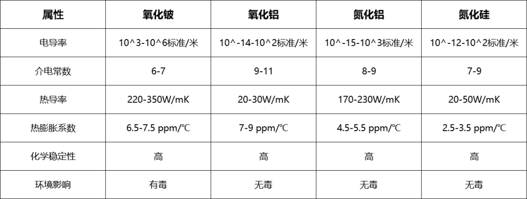
• Thermal Conductivity: The thermal conductivity of BeO is very high, ranging from 220 to 350 (W/mK). This thermal conductivity can rival that of metals, which is one of the main selling points of beryllium oxide.
2. Chemical Stability: BeO is a stable material at room temperature and is resistant to corrosion from chemicals such as acids and bases.
3. Electrical Properties
• Dielectric Constant: BeO has a low dielectric constant, ranging from 6 to 7. This is crucial when dealing with high-frequency signal propagation in PCBs, as it minimizes losses and enhances signal integrity.
• Volume Resistivity: BeO has relatively high volume resistivity, ranging from 10^14 to 10^16 ohm-centimeters. This makes BeO an excellent electrical insulator.
Disadvantages:
1. Cost
BeO is more expensive than most other substrate materials, leading many users to avoid it and resulting in a lack of manufacturing expertise among manufacturers.
2. Toxicity
As mentioned earlier, BeO releases toxic gases at 300°C as high temperatures cause it to decompose into boron oxide. Inhaling this substance can lead to chronic beryllium disease and lung cancer. Although it is not easy to reach 300°C in everyday life, high-temperature soldering is necessary during the PCB assembly process, which may reach this temperature, posing a serious risk to workers.
3. Limited Supply
BeO is a relatively rare material, and its reserves are not abundant, limiting the number of beryllium oxide ceramic PCBs that can be manufactured.
Is Beryllium Oxide Ceramic PCB
As mentioned earlier, beryllium oxide has many advantages such as thermal conductivity, reliability, and high-frequency applicability, but its most critical issue is toxicity.
Beryllium Oxide Ceramic PCB Manufacturing Process
1.Material Preparation
The main component of this process is beryllium oxide powder, which is measured, weighed, and quality assured to ensure compliance with specifications. Once prepared, the powder is mixed with a binder to form a slurry.
2.Shaping
The beryllium oxide slurry needs to be molded into sheets to create PCB substrates, using various methods to shape the slurry into its final form, including: dry pressing, injection molding, and extrusion.
3.Drying
The product obtained after shaping, also known as the green body, still contains liquid binder fluid that needs to be removed. The shaped slurry needs to be dried to form the desired beryllium oxide ceramic substrate. The green body is dried in a furnace, resulting in a porous white material that is brittle and needs to be handled with care.
4.Sintering
Sintering involves heating the fragile beryllium oxide to a temperature close to its melting point, typically above 1200°C. This causes the ceramic particles to fuse and produce a material with the desired properties that can be used as a substrate.
5.Machining
Machining involves using various mechanical machines to process the material into the final dimensions described by the designer in Gerber files and other production documents. These machining processes include: drilling, grinding, cutting, polishing, or precision machining using CNC machines.
6.Metalization
Once the beryllium oxide ceramic substrate is formed, it can be made into a PCB by adding conductive materials to the surface. Thin layers of conductive materials, such as metals like copper, gold, and silver, are used. This conductive layer will form the conductive traces connecting the various components of the PCB.
7.Electroplating and Etching
Electroplating is the process of adding a conductive layer on top of the existing conductive layer to enhance the material’s solderability and conductivity. The electroplated material is usually thinner than the underlying material and has better conductivity.
On the other hand, etching is the process of precisely creating individual conductive traces. This step enhances the performance of the PCB and ensures it meets the precision expected by the designer.
8.Surface Treatment
Once all conductive traces and plating layers are added, the PCB is essentially ready. Surface treatment of the PCB is performed on the exposed conductive materials.
The three main functions of surface treatment are: to prevent corrosion caused by oxidation, to improve solderability, and to provide a flat surface for the connection of surface-mounted components.
Some of the most common surface treatment techniques for PCBs include:
• Immersion Gold: This surface treatment consists of a layer of chemical nickel and a thin layer of immersion gold. This method offers excellent solderability and a very flat surface.
• HASL: This surface treatment is achieved by applying molten solder to the surface of the PCB, then using hot air to flatten and remove excess solder. This is an old technique and is very cost-effective.
• Immersion Tin: This process involves immersing the PCB in molten tin. This forms a thin layer of tin on the exposed pads. Tin has excellent solderability and a flat surface.
9.Inspection and Testing
Beryllium oxide ceramic PCBs are ready and need to undergo defect testing to ensure they meet customer requirements. The testing process is primarily automated and uses automated visual inspection equipment and automated test benches to test the continuity of all traces.
Source: Zhan Zhi Technology
Disclaimer: Some of the graphic and textual materials on this platform are sourced from the internet or provided by companies. If there is any infringement, please notify us, and we will verify and delete it immediately.
Advertisement
Not related to the content