▼Click the business card below to follow our public account ▼Layout
In design, layout is an important step. The quality of the layout directly affects the wiring results, so it can be said that a reasonable layout is the first step to successful PCB design.
Especially pre-layout, which is the process of considering the entire circuit board, signal flow, heat dissipation, structure, and other architectures. If the pre-layout fails, all subsequent efforts will be in vain.
1. Consider the Overall The success of a product depends on both its internal quality and overall aesthetics; both must be relatively perfect for the product to be considered successful. On a PCB, the layout of components should be balanced, orderly, and not top-heavy or bottom-heavy.
Will the PCB deform?
Are there reserved process edges?
Are there reserved MARK points?
Is panelization needed?
How many layers can ensure impedance control, signal shielding, signal integrity, economy, and feasibility?
2. Eliminate Basic Errors Does the PCB size match the processing drawing size? Can it meet PCB manufacturing process requirements? Are there positioning marks? Are there any conflicts between components in two-dimensional or three-dimensional space? Is the component layout orderly and neat? Is everything laid out? Can frequently replaced components be easily replaced? Is it convenient to insert the plug-in board into the device? Is there an appropriate distance between thermal-sensitive components and heat-generating components? Is it convenient to adjust adjustable components? Are heat sinks installed where heat dissipation is needed? Is air flow unobstructed? Is the signal flow smooth and the interconnections the shortest? Are plugs, sockets, etc., in conflict with mechanical design? Has the interference problem of the circuit been considered?
3. Bypass or Decoupling Capacitors
When wiring, both analog and digital devices require these types of capacitors, which need to be connected close to their power pins with a bypass capacitor, typically valued at 0.1μF. The leads should be as short as possible to reduce inductance, and they should be placed as close to the device as possible.
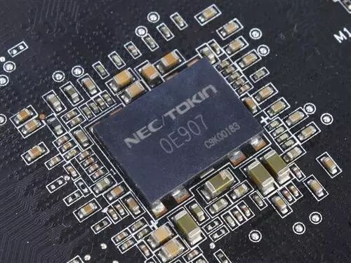
Adding bypass or decoupling capacitors on the circuit board, as well as their arrangement, is basic knowledge for both digital and analog designs, but their functions differ. In analog wiring design, bypass capacitors are typically used for bypassing high-frequency signals on the power supply; without them, these high-frequency signals may enter sensitive analog chips through the power pins. Generally, the frequency of these high-frequency signals exceeds the ability of analog devices to suppress them. If bypass capacitors are not used in analog circuits, noise may be introduced into the signal path, and in severe cases, it may even cause oscillation. For digital devices like controllers and processors, decoupling capacitors are also needed, but for different reasons. One function of these capacitors is to act as a “micro” charge reservoir because switching states in digital circuits often require large currents. When switching occurs, transient currents generated on the chip flow through the circuit board, and having this extra “reserve” charge is beneficial. If there is not enough charge during switching, it can cause significant voltage changes. Excessive voltage changes can lead to uncertain digital signal levels and may cause state machines in digital devices to malfunction. The switching current flowing through the circuit board traces will cause voltage changes, and due to parasitic inductance in the traces, the voltage change can be calculated using the formula: V=Ldl/dt where V=voltage change, L=trace inductance, dI=current change through the trace, dt=time of current change. Therefore, for various reasons, applying bypass (or decoupling) capacitors at the power supply or at the power pins of active devices is a very good practice.
4. Input Power, if the current is relatively large, it is recommended to reduce the trace length and area, and not to run full board.
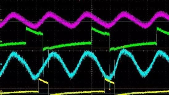
Switching noise on the input couples to the power output plane.Outputpower’sMOSswitching noise affects the input power of the previous stage.
If there are large current DCDC converters on the circuit board, there will be interference from different frequencies and large current high voltage transitions.
Therefore, we need to reduce the area of the input power supply to meet the current flow requirements. Thus, when laying out the power supply, we should consider avoiding running the input power supply across the entire board.
 5. Power and Ground Lines
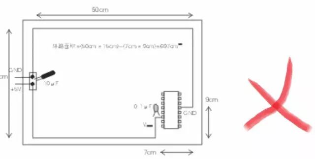
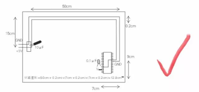
The proper positioning of power and ground lines can reduce the possibility of electromagnetic interference (EMI). If the power and ground lines are not properly matched, system loops may be created, which can likely generate noise. An example of improper PCB design with power and ground lines is shown in the figure. On this circuit board, different routes are used for power and ground lines, and due to this improper matching, the electronic components and traces on the PCB are more susceptible to electromagnetic interference (EMI).
 6. Separation of Digital and Analog
In every PCB design, the noisy parts of the circuit and the “quiet” parts (non-noisy parts) should be separated. Generally, digital circuits can tolerate noise interference and are not sensitive to noise (because digital circuits have a large voltage noise tolerance); in contrast, analog circuits have a much smaller voltage noise tolerance. Among the two, analog circuits are most sensitive to switching noise. In mixed-signal system wiring, these two types of circuits should be separated.
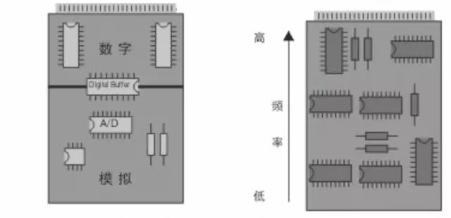 The basic knowledge of PCB wiring applies to both analog and digital circuits. A basic rule of thumb is to use a continuous ground plane, which reduces the dI/dt (current change over time) effect in digital circuits, as the dI/dt effect can cause ground potential and introduce noise into the analog circuit. The wiring techniques for digital and analog circuits are fundamentally the same, with one exception. For analog circuits, an additional point to note is to keep digital signal lines and return loops in the ground plane as far away from the analog circuit as possible. This can be achieved by connecting the analog ground plane separately to the system ground connection point or placing the analog circuit at the far end of the circuit board, which is the end of the traces. This is to minimize external interference on the signal path. Digital circuits do not require this, as they can tolerate a lot of noise on the ground plane without issue.
7. Heat Dissipation Considerations
During the layout process, it is necessary to consider heat dissipation pathways and dead corners; sensitive thermal components should not be placed behind heat sources. Priority should be given to the layout position of components like DDR that are difficult to dissipate heat. Avoid repeated adjustments due to thermal simulation failures.
Wiring
In PCB design, wiring is an important step in completing product design; it can be said that all previous preparatory work is done for it. In the entire PCB, the wiring design process is the most limited, with the finest techniques and the largest workload.
PCB wiring can be single-sided, double-sided, or multi-layered. There are two methods of wiring: automatic wiring and interactive wiring. Before automatic wiring, interactive wiring can be used to pre-wire lines with stricter requirements, and the edge lines of the input and output should avoid being parallel to each other to prevent reflection interference. Ground isolation should be added when necessary, and the wiring of adjacent layers should be perpendicular to each other, as parallel wiring can easily cause parasitic coupling.
The wiring rate of automatic wiring depends on good layout; wiring rules can be pre-set, including the number of bends in the traces, the number of vias, the number of steps, etc. Generally, exploratory wiring is done first to quickly connect short lines, followed by maze wiring, which optimizes the global wiring path for the lines to be wired. It can disconnect already wired lines as needed and attempt to rewire to improve overall performance.
Currently, high-density PCB designs have found that through-hole vias are not very suitable, as they waste a lot of valuable wiring channels. To solve this contradiction, blind and buried via technologies have emerged, which not only fulfill the role of through-hole vias but also save many wiring channels, making the wiring process more convenient, smoother, and more complete. The PCB design process is a complex yet simple process; to master it well, electronic engineering designers need to experience it themselves to grasp its essence.
1. Handling of Power and Ground Lines
Even if the wiring throughout the PCB is well done, interference caused by inadequate consideration of power and ground lines can degrade product performance and sometimes even affect product success rates. Therefore, the wiring of power and ground lines must be taken seriously to minimize noise interference generated by power and ground lines, ensuring product quality.
Every engineer engaged in electronic product design understands the causes of noise generated between ground and power lines. Here, we only describe the methods to reduce noise suppression:
(1) It is well known to add decoupling capacitors between power and ground lines.(2) Try to widen the power and ground line widths; it is best if the ground line is wider than the power line. Their relationship is: ground line > power line > signal line. Typically, the signal line width is: 0.2 to 0.3mm, with the thinnest width reaching 0.05 to 0.07mm, and the power line is 1.2 to 2.5mm. For digital circuit PCBs, wide ground conductors can form a loop, i.e., forming a ground network for use (the ground of the analog circuit cannot be used this way).(3) Use large copper areas as ground lines, connecting all unused areas on the printed board to ground. Alternatively, make it a multi-layer board, with power and ground lines occupying one layer each.
2. Common Ground Handling for Digital and Analog Circuits
Now many PCBs are no longer single-function circuits (digital or analog) but are composed of mixed digital and analog circuits. Therefore, when wiring, it is necessary to consider the interference issues between them, especially the noise interference on the ground line.
Digital circuits have high frequencies, while analog circuits are highly sensitive. For signal lines, high-frequency signal lines should be kept as far away as possible from sensitive analog circuit components. For ground lines, the PCB has only one node to the outside world, so the common ground issue between digital and analog circuits must be handled internally on the PCB. Internally, the digital ground and analog ground are actually separated and not connected to each other, only at the interface connecting the PCB to the outside (such as plugs, etc.). There should be only one connection point between the digital ground and analog ground. There are also cases where the PCB does not share a ground, which is determined by system design.
3. Signal Lines on Power (Ground) Layers
When wiring on multi-layer printed boards, if there are not many remaining lines on the signal line layer, adding more layers will cause waste and increase the workload for production, which will also increase costs. To solve this contradiction, consider wiring on the power (ground) layer. First, consider using the power layer, and then the ground layer, as it is best to maintain the integrity of the ground layer.
4. Handling of Connection Legs in Large Area Conductors
In large area grounds (power), the connection of commonly used component legs needs to be considered comprehensively. From an electrical performance perspective, the solder pads of component legs should be fully connected to the copper surface, but there are some adverse hidden dangers for component soldering assembly, such as: (1) Soldering requires a high-power heater. (2) It is easy to create cold solder joints. Therefore, balancing electrical performance and process needs, a cross-shaped solder pad is made, known as a heat shield, commonly referred to as a thermal pad. This greatly reduces the possibility of cold solder joints caused by excessive heat dissipation during soldering. The treatment of connection legs in multi-layer boards is the same.
5. Role of Network Systems in Wiring
In many CAD systems, wiring is determined by the network system. A dense grid increases the number of pathways, but if the steps are too small, the data volume of the drawing will have higher requirements for the device’s storage space and will greatly affect the computation speed of computer electronic products. Some pathways are ineffective, such as those occupied by component leg pads or installation holes, positioning holes, etc. A sparse grid with too few pathways greatly affects the wiring rate. Therefore, a reasonably dense grid system is needed to support the wiring process.
The standard distance between two legs of standard components is 0.1 inches (2.54mm), so the basic grid system is generally set to 0.1 inches (2.54mm) or an integer multiple less than 0.1 inches, such as: 0.05 inches, 0.025 inches, 0.02 inches, etc.
6. Design Rule Check (DRC)
After completing the wiring design, it is necessary to carefully check whether the wiring design meets the rules set by the designer and also confirm whether the rules meet the requirements of the printed board production process. Generally, the checks include the following aspects:
(1) Are the distances between lines, lines and component pads, lines and vias, component pads and vias, and vias and vias reasonable and meet production requirements?(2) Are the widths of power and ground lines appropriate? Are the power and ground lines tightly coupled (low wave impedance)? Is there any place in the PCB that allows the ground line to be widened?(3) Have the best measures been taken for critical signal lines, such as the shortest length, protective lines, and clear separation of input and output lines?(4) Do the analog and digital circuit sections have their own independent ground lines?(5) Will graphics added to the PCB (such as icons, annotations) cause signal short circuits?(6) Are there any undesirable line shapes that need to be modified?(7) Are there any process lines added to the PCB? Does the solder mask meet production process requirements, is the solder mask size appropriate, and are character marks pressed on component pads to avoid affecting assembly quality?(8) In multi-layer boards, is the outer edge of the power ground layer reduced, as exposed copper foil from the power ground layer can easily cause short circuits?
7. Check for Sharp Corners, Impedance Discontinuities, etc.
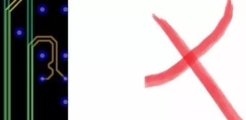
(1) For high-frequency currents, when the bends of the wires are right angles or even sharp angles, the magnetic flux density and electric field strength near the bend are relatively high, which will radiate strong electromagnetic waves, and the inductance at this point will be larger than that of obtuse or rounded corners.
(2) For the bus wiring of digital circuits, the bends should be obtuse or rounded, as the area occupied by the wiring is relatively small. Under the same line spacing conditions, the total line spacing occupied by the width of the lines with right-angle bends is 0.3 times less.
8. Check the 3W and 3H Principles
(1) Clock, reset, signals above 100M, and some key bus signals must meet the 3W principle, with no long parallel traces on the same layer and adjacent layers, and as few vias as possible on the link.
(2) The number of vias for high-speed signals is a strict requirement in some device manuals. The principle of interconnection is that in addition to the necessary pin fanout vias, no extra vias should be drilled in the inner layers. They have routed 8G PCIE 3.0 traces with only 4 vias without issues.
(3) The center distance of clock and high-speed signals on the same layer must strictly meet the 3H (H is the distance from the routing layer to the return plane); signals on adjacent layers must not overlap, and it is recommended to also meet the 3H principle. There are tools available to check the aforementioned crosstalk issues.
Wiring Constraints
Wiring Constraints: Layer Distribution Wiring Constraints: Layer Distribution
Each layer of RF PCB has a large area of auxiliary ground, with no power plane. The layers adjacent to the RF wiring layer should be ground planes. Even in mixed-signal boards, the digital part can have a power plane, but the RF area must still meet the requirement of having a large area of auxiliary ground on each layer.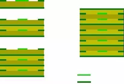
RF Single Board Layer Structure
Wiring Constraints: Basic Requirements
(1) Wiring should be as short as possible, avoiding closed loops and sharp right angles, with consistent line widths and no floating lines.
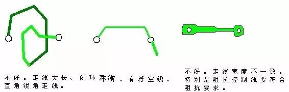 (2) The way pads are wired out should be reasonable.
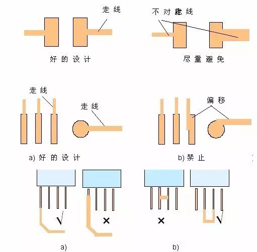 Basic Wiring Requirements Diagram
(3) Differential signal lines are generally high-speed signals that must meet impedance symmetry; differential lines must not cross each other, and the length difference must not exceed 100mil. The spacing between differential lines and between a single differential line and ground must meet impedance requirements. The number of vias for differential lines must not exceed 4. The spacing between differential lines must meet the 3W rule.
(4) General oscillators, PLL filter devices, analog signal processing chips, inductors, and transformers should not have clock lines, control lines, or electromagnetically sensitive lines running underneath them.
(5) Analog signals and digital signals, power lines and control signal lines, weak signals and any other signals must not run in parallel; they should be separated by layers (preferably with ground isolation) or run at a considerable distance apart. If adjacent layers’ lines must cross, they must not run in parallel. To reduce crosstalk between lines, ensure that the spacing between lines is sufficiently large; when the center-to-center spacing between lines is at least 3 times the line width, 70% of the electric field will not interfere with each other, known as the 3W rule. To achieve 98% of the electric field not interfering with each other, a 10W spacing should be used.
Note: When routing clock lines, be sure to pay attention to effective isolation from data lines and control signal lines; the farther apart, the better, and avoid routing them on the same layer as much as possible.
(6) Strong radiating signal lines (high frequency, high speed, especially clock lines) should not be close to interfaces, pull tabs, etc., to prevent external radiation.
(7) Sensitive signals (mainly referring to weak signals, reset signals, comparator input signals, reference power for AD, phase-locked loop filter signals, and filtering parts of PLL circuits inside chips) should be routed as short as possible, away from strong radiating signals, and not placed at the edge of the board, at least 15mm away from the outer metal frame. For long-distance routing, ground wrapping can be used (note that ground wrapping may cause impedance changes), and inner layer routing is recommended. Additionally, for chips with weak ESD protection, routing on inner layers is suggested to reduce the probability of chip damage.
Wiring Constraints: Power Supply
(1) Pay attention to power supply decoupling and filtering to prevent different units from generating interference through the power supply line; when wiring the power supply, the power lines should be isolated from each other. Power lines should be isolated from other strong interference lines (such as CLK) using ground lines.
(2) The power supply wiring for small signal amplifiers requires ground copper skin and grounding vias for isolation to avoid other EMI interference from entering, thereby degrading the signal quality of this stage.
(3) Different power supply layers should avoid overlapping in space. This is mainly to reduce interference between different power supplies, especially between power supplies with significant voltage differences. The issue of overlapping power planes must be avoided; if unavoidable, consider using an intermediate ground layer.
Wiring Constraints: Power Overcurrent Capability
(1) The printed lines in the power section must meet the current-carrying requirements for the number of vias (1A/Φ0.3mm hole).
(2) The copper foil size in the POWER section of the PCB must meet the maximum current flowing through it and consider a margin (generally referenced as 1A/mm line width).
Wiring Constraints: Grounding Methods
(1) Ground lines should be short and straight to reduce distributed inductance and minimize interference caused by common ground impedance.
Adjust the direction of filtering capacitors in each group to minimize ground loops. As shown in Figure 15, the three filtering capacitors should be grounded towards the relevant RF device direction, especially for high-frequency filtering capacitors.
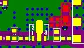 Grounding Diagram of Capacitors
(2) When grounding devices on the main RF signal path and power filtering capacitors, to reduce the grounding inductance of the devices, they should be grounded nearby.
(3) For some components with grounded metal shells on the bottom, add some grounding holes within the projection area of the components; no signal lines or vias should be routed in the surface layer within the projection area.
(4) When grounding lines need to run a certain distance, they should be widened, and the length of the lines should be shortened, prohibiting them from approaching or exceeding 1/4 of the guiding wavelength to prevent antenna effects that lead to signal radiation.
(5) Except for special purposes, there should be no isolated copper areas; grounding vias must be added to copper areas.
(6) For certain sensitive circuits and circuits with strong radiation sources, they should be placed in shielding cavities, and during assembly, the shielding cavity should press against the PCB surface. During PCB design, a “via shielding wall” should be added, which means adding grounding vias at the parts of the PCB that are in close contact with the shielding cavity wall. As shown in the figure, there should be more than two rows of vias, with the two rows staggered, and the spacing between vias in the same row should be about 100 mils.
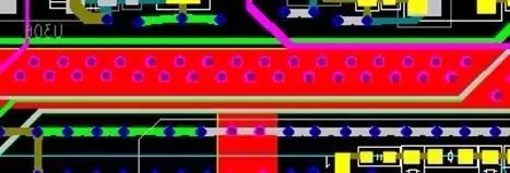
Wiring Constraints: General Rules
(1) RF signals should be routed on the top layer of the PCB, and the plane layer below the RF signal must be a complete ground plane, forming a microstrip line structure. As shown in Figure 13, to ensure the integrity of the microstrip line structure, the microstrip line must be treated with ground copper skin, and it is recommended that the edge of the ground copper skin be 3H away from the edge of the microstrip line. H represents the thickness of the dielectric layer. Within the 3H range, no other signal vias should be present. Non-coupled microstrip lines should have ground copper skin added, and grounding vias should be added to the ground copper skin.
The distance from the microstrip line to the shielding wall should be maintained at more than 3H. Microstrip lines should not cross the dividing line of the second layer ground plane.
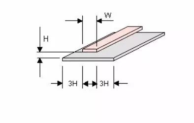
Microstrip Line Structure Diagram
(2) The spacing between ground copper skin and signal routing lines should be ≥3H.
(3) Ground copper skin edges should have grounding holes, with a spacing of about 100 mils, arranged uniformly and neatly.
(4) The edges of the ground copper skin should be smooth and flat, prohibiting sharp burrs.
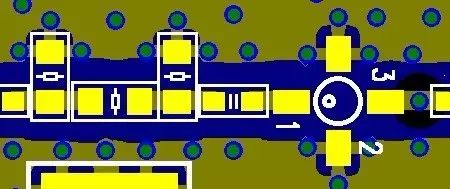 (5) Except for special purposes, RF signal lines should not have excess line ends protruding.
(6) If there are other RF signal lines around RF signal wiring, ground copper skin should be added between the two for isolation, and a grounding via should be added every 100 mils or so.
(7) If there are other unrelated non-RF signal lines (such as power lines) around RF signal wiring, ground copper skin should be added between the two, and a grounding via should be added every 100 mils or so.
(8) If RF signal vias are close to other wiring in the inner layer, such as the power line shown in the left figure, the EMI interference on the power line will invade the RF wiring. Therefore, the correct wiring method shown in the right figure should be used, adding ground copper skin and grounding vias between the power line and RF signal vias for isolation. Sometimes, RF signal lines in the inner layer are close to other signals with strong interference (such as power lines), and the same method of adding ground copper skin and grounding vias should be used for isolation.
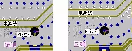 Wiring Diagram of Power Lines and RF Vias
(9) When the device installation hole is a non-metalized hole, RF signal wiring should be kept away from the device installation hole. Ground copper skin should be added between RF signal wiring and installation holes, along with grounding vias.
1. Wiring Priority Order
Key signal lines take priority: power, analog small signals, high-speed signals, clock signals, and synchronous signals are all key signals that should be prioritized in wiring.
The density priority principle: Start wiring from the components with the most complex connection relationships on the board. Begin wiring from the areas with the densest connections on the board.
2. Automatic Wiring
When the wiring quality meets design requirements, automatic wiring tools can be used to improve work efficiency. Before automatic wiring, the following preparatory work should be completed:
Automatic wiring control file (do file) To better control wiring quality, it is generally necessary to define wiring rules in detail before running. These rules can be defined in the software’s graphical interface, but the software provides better control methods, namely writing an automatic wiring control file (do file) based on the design situation, under which the software operates.
3. Try to provide dedicated wiring layers for clock signals, high-frequency signals, sensitive signals, and other key signals, ensuring their minimum loop area.
When necessary, manual priority wiring, shielding, and increasing safety spacing methods should be adopted to ensure signal quality.
4. The EMC environment between power layers and ground layers is poor, and sensitive signals should be avoided.
5. Networks with impedance control requirements should be routed on impedance control layers.
6. Rules to Follow During PCB Design
1) Ground loop rules: The minimum loop rule states that the area formed by the signal line and its loop should be as small as possible; the smaller the loop area, the less radiation to the outside, and the less interference received from the outside. Regarding this rule, when dividing the ground plane, consider the distribution of the ground plane and important signal traces to prevent issues caused by ground plane slots; in double-layer board design, while leaving enough space for power, the remaining part should be filled with reference ground, and some necessary vias should be added to effectively connect the double-sided ground signals. For some key signals, ground isolation should be used as much as possible, and for some high-frequency designs, special consideration should be given to the ground plane signal loop issues, and multi-layer boards are recommended.
2) Crosstalk control: Crosstalk refers to the mutual interference caused by long parallel wiring between different networks on the PCB, mainly due to the distributed capacitance and inductance between parallel lines. The main measures to overcome crosstalk are:
Increase the spacing between parallel wires, following the 3W rule.
Insert grounding isolation lines between parallel lines.
Reduce the distance between the wiring layer and the ground plane.
3) Shielding Protection
Corresponding to the ground loop rules, this is actually also to minimize the signal loop area, often seen in some important signals, such as clock signals and synchronous signals; for particularly important signals with very high frequencies, consider using a copper shield cable structure design, i.e., isolating the routed line with ground lines on all sides, and also considering how to effectively combine the shield ground with the actual ground plane.
4) Control of Wiring Direction Rules:
This means that the wiring direction of adjacent layers should be orthogonal. Avoid routing different signal lines in the same direction on adjacent layers to reduce unnecessary inter-layer interference; when this situation is unavoidable due to board structure limitations (such as certain backplanes), especially when the signal rate is high, consider using ground planes to isolate each wiring layer and using ground signal lines to isolate each signal line.
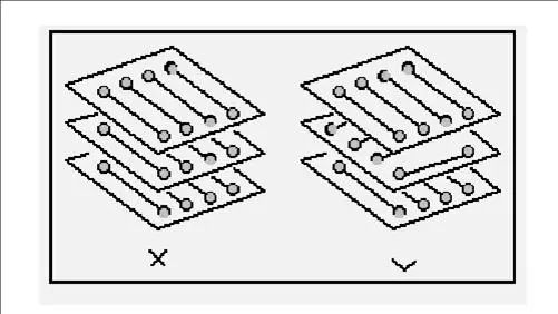
5) Open Loop Check Rules for Wiring:
Generally, wiring with one end floating (Dangling Line) is not allowed, mainly to avoid generating the “antenna effect” and reduce unnecessary interference radiation and reception, otherwise it may lead to unpredictable results.
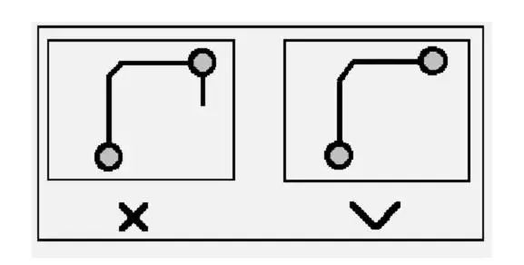
6) Impedance Matching Check Rules:
The wiring width of the same network should remain consistent; changes in line width will cause uneven characteristic impedance of the line, which can lead to reflections when the transmission speed is high. This situation should be avoided as much as possible in design. Under certain conditions, such as lead wires for connectors or BGA package lead wires with similar structures, changes in line width may be unavoidable, and the effective length of the inconsistent parts should be minimized.
7) Line Termination Network Rules:
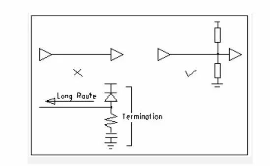
In high-speed digital circuits, when the delay time of PCB wiring is greater than 1/4 of the signal rise time (or fall time), the wiring can be considered a transmission line. To ensure that the input and output impedance of the signal matches the transmission line impedance correctly, various matching methods can be used, and the chosen matching method depends on the network’s connection method and the topology of the wiring.
A. For point-to-point (one output corresponds to one input) connections, series matching at the start or parallel matching at the end can be chosen. The former is simple and low-cost but has a larger delay. The latter has better matching effects but is more complex and costly.
B. For point-to-multipoint (one output corresponds to multiple outputs) connections, when the network topology is a daisy chain, terminal parallel matching should be chosen. When the network is star-shaped, point-to-point structure can be referenced.
Star and daisy chain are two basic topological structures; other structures can be considered variations of the basic structure, and some flexible measures can be taken for matching. In practical operations, cost, power consumption, and performance should be balanced; generally, complete matching is not pursued, as long as the reflections and other interferences caused by mismatching are limited to an acceptable range.
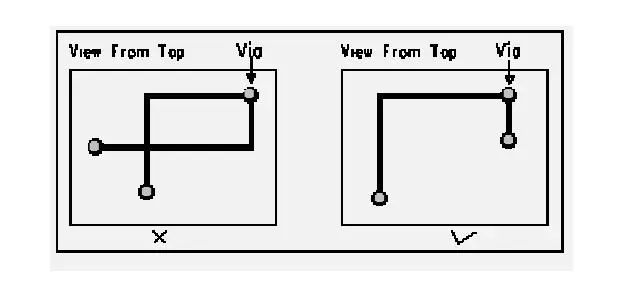
8) Loop Closure Check Rules for Wiring:
Prevent signal lines from forming self-loops between different layers. This issue is easy to occur in multi-layer board designs, and self-loops will cause radiation interference.
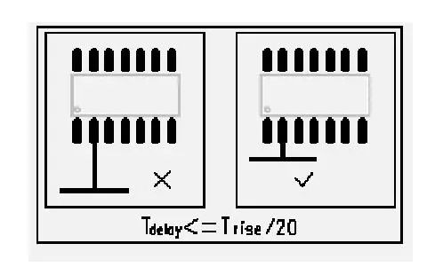
9) Control of Branch Length Rules for Wiring:
Try to control the length of branches; the general requirement is Tdelay<=Trise/20.
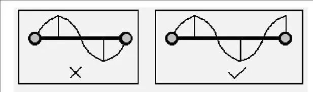
10) Resonance Rules for Wiring:
This mainly applies to high-frequency signal designs, where the wiring length should not be an integer multiple of its wavelength to avoid resonance phenomena.
11) Control of Wiring Length Rules:
This is the short line rule; in design, the wiring length should be kept as short as possible to reduce interference issues caused by excessive wiring length, especially for important signal lines such as clock lines. The oscillator should be placed very close to the device. For situations where multiple devices are driven, the specific network topology should be determined based on the situation.
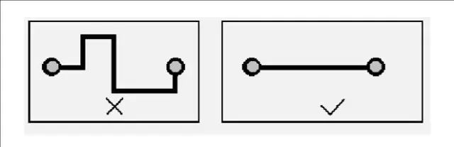
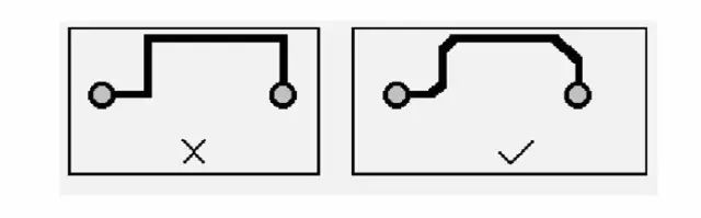
12) Chamfering Rules:
PCB design should avoid sharp angles and right angles to prevent unnecessary radiation, and the process performance is also poor.
13) Component Decoupling Rules:
A. Add necessary decoupling capacitors on the printed board to filter out interference signals on the power supply, stabilizing the power supply signal. In multi-layer boards, the position of decoupling capacitors is generally not too high, but for double-layer boards, the layout of decoupling capacitors and the wiring method of the power supply will directly affect the stability of the entire system, sometimes even determining the success or failure of the design.
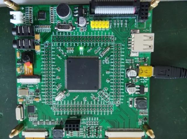
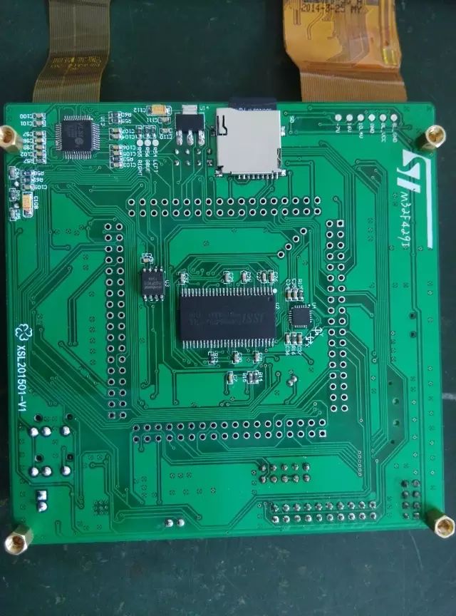
B. In double-layer board design, the current should generally pass through filtering capacitors before being used by devices, and the impact of power noise generated by devices on downstream devices should be fully considered. Generally, a bus structure design is better, and during design, the impact of voltage drop caused by excessive transmission distance on devices should be considered, and power filtering loops should be added when necessary to avoid potential differences.
C. In high-speed circuit design, the correct use of decoupling capacitors is crucial for the stability of the entire board.
14) Component Layout Partitioning/Layering Rules:
A. This is mainly to prevent mutual interference between modules operating at different frequencies while minimizing the wiring length of high-frequency parts. Typically, high-frequency parts are placed at the interface to reduce wiring length; of course, this layout still needs to consider potential interference from low-frequency signals. Additionally, the issue of separating ground planes for high/low frequency parts should be considered, usually by separating the two grounds and connecting them at a single point at the interface.
B. For mixed circuits, analog and digital circuits are often arranged on opposite sides of the printed board, using different layers for wiring, with ground layers isolating them.
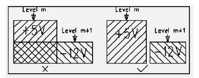
15) Control Rules for Isolated Copper Areas:
The emergence of isolated copper areas will bring some unpredictable problems; therefore, connecting isolated copper areas with other signals helps improve signal quality. Typically, isolated copper areas are grounded or removed. In actual production, PCB manufacturers add some copper foil to the vacant parts of some boards, mainly to facilitate PCB processing and also to prevent PCB warping.
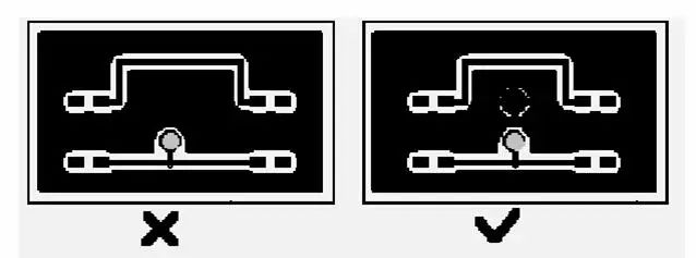
The emergence of isolated copper areas will bring some unpredictable problems; therefore, connecting isolated copper areas with other signals helps improve signal quality.
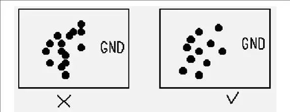
Typically, isolated copper areas are grounded or removed. In actual production, PCB manufacturers add some copper foil to the vacant parts of some boards, mainly to facilitate PCB processing and also to prevent PCB warping.
16) Integrity Rules for Power and Ground Layers:
For areas with dense vias, care should be taken to avoid vias connecting in the hollow areas of power and ground layers, which would disrupt the integrity of the plane layers and increase the return area of signal lines in the ground layer.
17) Overlapping Power and Ground Layer Rules:
Different power supply layers should avoid overlapping in space. This is mainly to reduce interference between different power supplies, especially between power supplies with significant voltage differences. The issue of overlapping power planes must be avoided; if unavoidable, consider using an intermediate ground layer.
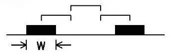
18) 3W Rule:
To reduce crosstalk between lines, ensure that the spacing between lines is sufficiently large; when the center-to-center spacing between lines is at least 3 times the line width, 70% of the electric field will not interfere with each other, known as the 3W rule. To achieve 98% of the electric field not interfering with each other, a 10W spacing should be used.
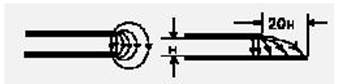
 19) 20H Rule:
Due to the changing electric field between power and ground layers, electromagnetic interference radiates outward at the edges of the board, known as edge effects. The solution is to retract the power layer, ensuring that the electric field only conducts within the range of the ground layer. By retracting 20H (where H is the thickness of the dielectric between power and ground), 70% of the electric field can be confined within the edge of the ground layer; retracting 100H can confine 98% of the electric field.
20) Five-Five Rule:
The rule for selecting the number of layers in printed boards states that if the clock frequency is up to 5MHz or the pulse rise time is less than 5ns, the PCB must use a multi-layer board. This is a general rule; sometimes, due to cost and other factors, a double-layer board structure is used. In this case, it is best to make one side of the printed board a complete ground plane layer.
Statement: This account maintains neutrality regarding all original and reprinted articles’ statements and viewpoints. The articles and images’ copyrights belong to the original authors. If there is any infringement, please contact us for deletion.

 【Tutorial】Electronic Components【Tutorial】Fundamentals of Analog Electronics【Tutorial】Fundamentals of Digital Electronics【Tutorial】Circuit Theory
【Tutorial】Electromagnetic Compatibility
【Tutorial】Microcontroller Principles and Applications
【Tutorial】C Language Basics
【Tutorial】Real-Time Operating System uCOS-II
【Tutorial】ARM Basics
【Resources】20 Smart Home System Design Resources
【Resources】400+ Electronic Circuit Animated Courseware + 147G Hardware Design and Development Video Resources
【Resources】100+ Switching Power Supply Design Resources
【Resources】800+ Microcontroller Design Resources, Mastering Microcontroller Circuit Design~
【Resources】10G+ AD Package Library Files, Meeting 99% of Your Development Needs!
【Resources】60+ Inverter Power Supply Resources, Supporting New Energy Application Development
【Resources】31 Automatic Calculation Formula Tables for Flyback Parameters
【Resources】176 Power MOSFET Circuit Learning Resources
【Resources】97 Switching Power Supply Loop Control Design Resources
【Resources】525 Microcontroller C Language Simulation Examples
【Resources】5 Sets of DC Brushless Three-Phase Motor Control Solutions
【Resources】1399 Cadence PCB Operation Manual Package Library Files

 Read the original text to get more learning resources