
Printed Circuit Boards (PCBs) are ubiquitous in electronic devices and other related applications. Generally, PCBs are made of multiple layers of laminated materials and resin bonded together. These layers embed conductive metal components and metal vias that pass vertically through these layers.
In Finite Element Analysis (FEA), the body and traces in a PCB are typically modeled as elements using solid, shell, and beam elements with coupling or contact. However, due to the enormous number of embedded bodies involved in each resin layer of the PCB, this approach is often difficult and time-consuming.
Mesh-independent enhanced element technology allows for the definition of the topology of embedded regions using MESH200 elements, seamlessly creating embedded enhanced elements, providing better options for modeling and meshing PCBs. This does not involve complex contact modeling, coupling, or difficult meshing techniques.
This example problem demonstrates how to perform thermal structural analysis of a Printed Circuit Board (PCB) using mesh-independent enhanced elements.
Key features and functionalities highlighted include:
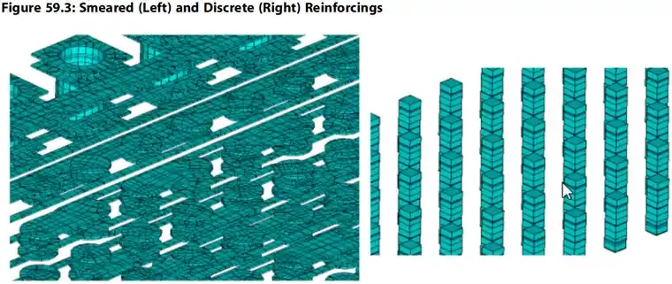
Modeling using discrete and smeared reinforcement elements.
Performing downstream structural analysis after thermal analysis.
Description of the problem:
The analysis is divided into two parts:
Step 1. Solving thermal analysis caused by thermal boundary conditions.
Step 2. Resolving downstream structural analysis caused by thermal loads.
Heat generated by running loads on some embedded metal traces can cause temperature gradients across the entire PCB. The gradients can cause the PCB to deform during operation, leading to thermal stress and strain.
Modeling
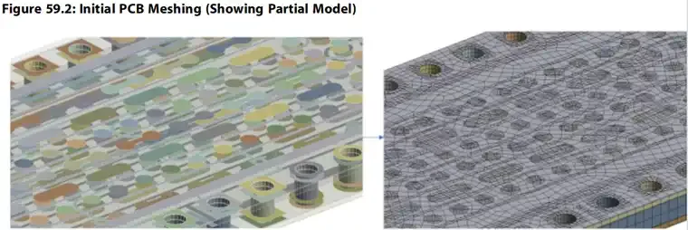
The model for steady-state thermal analysis is created using ANSYS Mechanical, generating the initial mesh of elements:
The line body representing small copper vias is meshed using LINK33.
Other surface bodies representing copper embedded in resin and larger vias are meshed using SHELL131.
The laminated and resin solids are meshed using SOLID70. The SOLID70 elements are modified (EMODIF) to create SOLID278 elements to support the generation of enhanced elements.
Each solid laminate and resin body defaults to bonded contact at their inner surfaces, forming six bonded contact pairs.
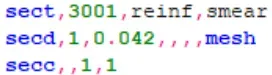
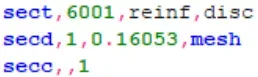
To create embedded reinforcement elements (REINF264 and REINF265), LINK33 and SHELL131 elements are modified (EMODIF) to create equivalent MESH200 elements.
The smeared reinforcement with a thickness of 0.042 mm has the following cross-sectional properties:
The discrete reinforcement with a cross-sectional area of 0.16053 mm2 has the following cross-sectional properties:
After selecting appropriate base SOLID278 and MESH200 elements, reinforcement components (EREINF) are created and shaped (/ESHAPE):
For downstream structural analysis, the SOLID278 elements are modified (EMODIF) to create equivalent SOLID185 elements. As part of the thermal contact pair, the CONTA174 elements are also modified to account for the structural solution. The reinforcement elements REINF264 and REINF265 are then reselected to achieve their structural degrees of freedom (EREINF).
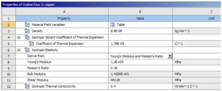
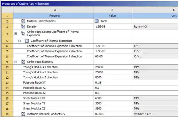
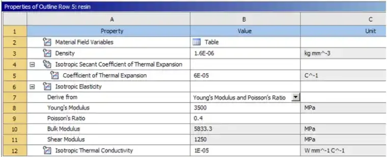
Material Properties
The following are the thermal and structural material properties of copper, laminated materials, and resin materials at 22°C:
Boundary Conditions and Loading
Steady-State Thermal Analysis: Boundary Conditions and Loading
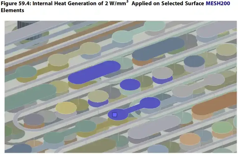
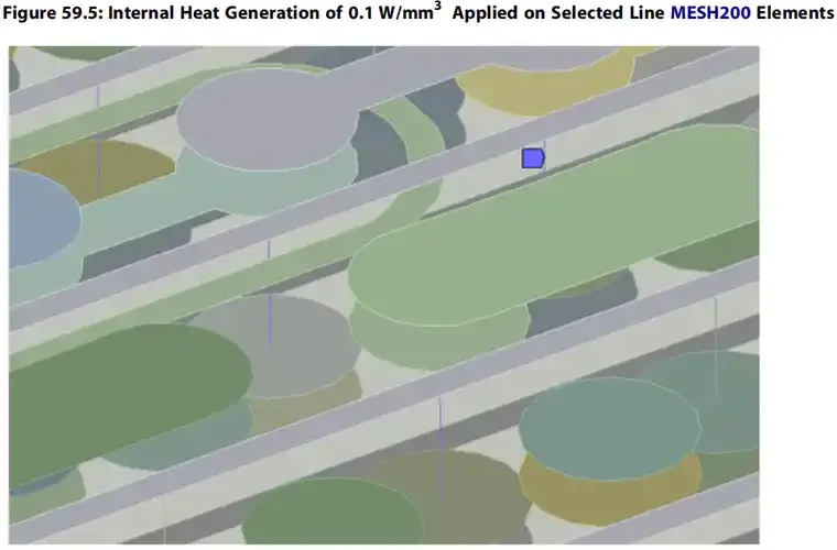
Internal heat loads are applied to selected MESH200 elements representing embedded copper traces and vias:
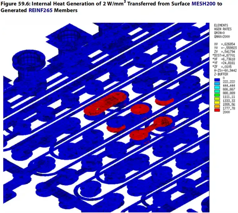
After creating the reinforcement (EREINF) from the intersection of MESH200 and base components, the boundary conditions applied to MESH200 are transferred to the smeared reinforcement components (BFPORT):
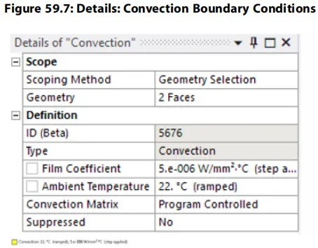
Convective boundary conditions are applied to the top and bottom surfaces of the PCB:

Downstream Structural Analysis: Boundary Conditions and Loading
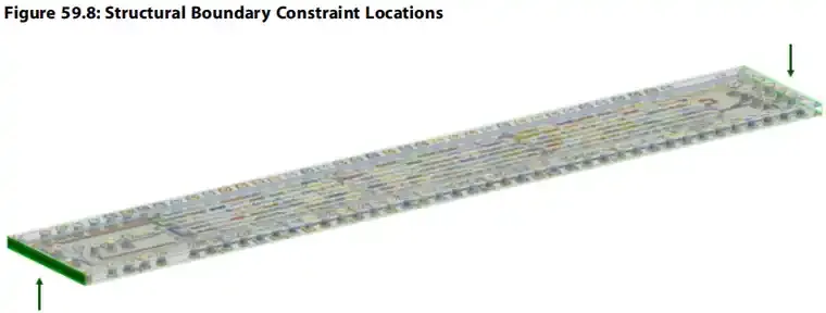
The ends of the PCB are constrained in all displacement degrees of freedom (shown in green):
Analysis and Solution Control
This solution includes steady-state thermal analysis and downstream structural analysis.
After applying thermal generation loads and convective boundary conditions, the steady-state thermal solution is straightforward.
The subsequent structural solution involves reading temperatures from the .rth file (LDREAD).
By defining at least five substeps, large deflections can be achieved.
Displacement convergence is enabled, while thermal flow convergence is disabled (CNVTOL). Before solving the structural analysis, previously defined convective SURF152 elements are deselected.
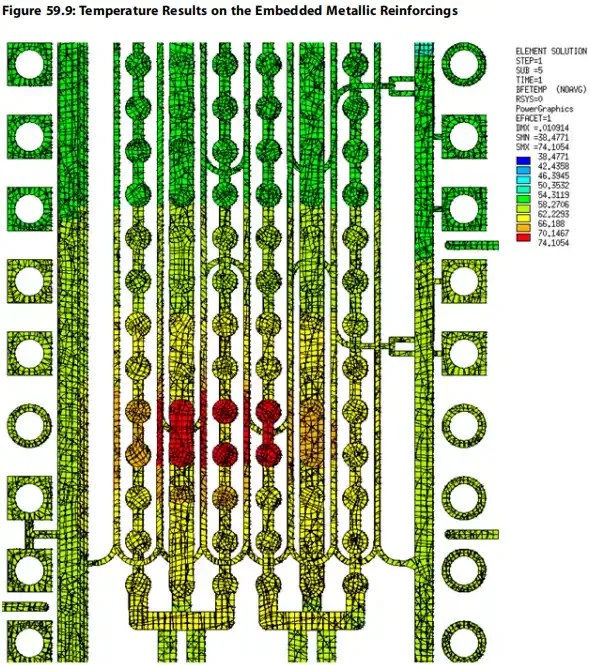
Results and Discussion
After the steady-state thermal analysis, the temperature results are of utmost importance. Below are the results for some smeared reinforcement:
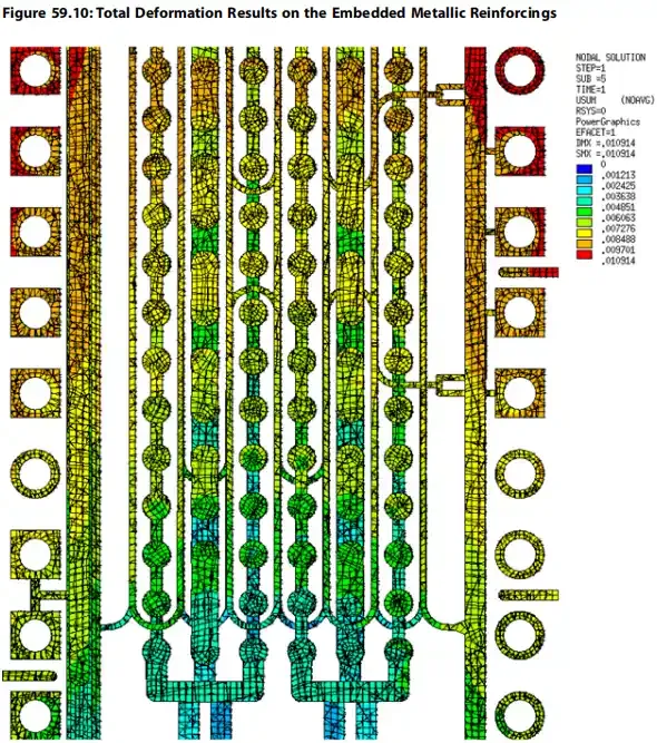
The temperature gradient leads to deformation and stress in the downstream structural analysis.
Below are the deformation results for the same part of the smeared reinforcement:
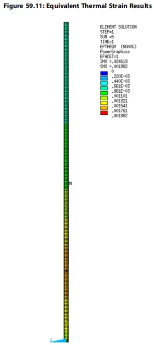
The equivalent thermal strain map of the entire PCB (viewed from the positive X axis) shows that strain occurs at expected locations and corresponds to the loading conditions of the thermal analysis:
The pore pressure distribution differs in some aspects from the results in the literature when conducting similar analyses. Consider the following tips and recommendations:
Choose sufficiently large sizes for solid base elements to avoid overly fine base meshes. If the base elements are smaller than the cross-section or thickness of the embedded components, the thermal generation loads may not be adequately distributed, leading to overestimation of thermal results in the affected areas.
Use appropriate cross-section control settings (SECCONTROL) for reinforcement elements to improve results.
Consider using the substrate removal option for all supporting base materials and full membrane options for homogeneous embedded components.

Screenshots from the eBook
【Complete Set of Hardware Learning Materials】