With the significant improvement in the processing capabilities of communication devices, whether designing computer systems, next-generation semiconductor products, or communication systems, RF engineers must cope with increasingly higher signal rates. To enable high-speed devices to process data more efficiently, they have tirelessly invented technologies that can increase external bus bandwidth, allowing for the transmission of large amounts of data between circuit board devices via backplanes or cables.
Increasing the signal frequency is one method to enhance bus bandwidth. This is because raising the signal frequency can reduce the rise time of digital signals. Poor-quality oscilloscope probes can cause overshoot and ringing in the measured waveforms of these signals with rapid rise times. Engineers must determine whether these anomalies are present in the design and whether they are caused by the measurement system.When transmitting data at high speeds, the contact between the oscilloscope probe and the circuit under test can introduce parasitic effects, leading to significant anomalies in the measured waveform. Additionally, the probe may add load to the circuit, causing the signal to change significantly or become distorted. Therefore, a thorough understanding of how the oscilloscope probe affects the circuit under test and the measured waveform will significantly improve measurement results.
Oscilloscope probe input impedance
Oscilloscope designers have made great strides in improving sampling rates, bandwidth, and accuracy. To achieve optimal performance in specific applications, careful selection and operation of oscilloscope probes are essential. However, the importance of accessories is often overlooked. Probes are the primary connection tool between the circuit under test and the oscilloscope. They can affect measurement results and the operation of the circuit under test.
When the probe connects to the circuit under test, it effectively adds a load to that circuit. This probe load consumes additional signal source current, altering the operating conditions of the circuit after the test point, thereby changing the measured signal.
To obtain accurate measurement results, the probe must capture the signal and provide the most accurate signal display without adding extra load or altering the signal source within its frequency range. In practice, all probes will add a complex load to the circuit under test (see Figure 1). Therefore, when selecting a probe, it is crucial to limit this load value to an acceptable range.
Probe specifications list input impedance and capacitance. These two factors combined can alter the circuit under test and add load to it. At low frequencies, the capacitor behaves like an open circuit, with DC resistance being the primary factor forming the circuit load. The resistive load is the least influential factor in probe loading because it does not produce nonlinear circuit characteristics.
Although excessive leakage current from low-impedance probes can cause nonlinear responses or disrupt circuit operation, the low-voltage, high-speed signal probes currently in use have largely resolved this issue.
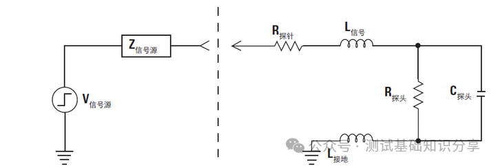
Figure 1. A simple input impedance model of an oscilloscope probe (including resistive, capacitive, and inductive components).
Oscilloscope probe input impedance
Assuming the signal source impedance is resistive, the resistive component of the probe will form a voltage divider (composed of the circuit output impedance and the probe input impedance), which can reduce the voltage amplitude of the measured signal without altering its shape (see Figure 2). The smaller the probe resistance relative to the signal source impedance, the more the probe load will reduce the voltage amplitude of the measured waveform. Additionally, the smaller the probe impedance relative to the circuit impedance, the greater the current flowing into the probe, increasing the likelihood of adverse effects on the circuit.
As the signal frequency increases or the edge speed decreases, the capacitive characteristics of the probe behave like a short circuit, allowing current to flow into the low-impedance probe. During the high-frequency phase of the signal, capacitive reactance becomes the primary factor contributing to circuit load, potentially causing circuit failure, as the circuit may not drive sufficient voltage headroom at this time.
Capacitive load is the main source of measurement errors related to the probe, as it affects rise and fall times, bandwidth, and edge-to-edge time measurements. Capacitive load can alter the shape of the measured waveform by inducing exponential responses (Figure 3), thereby eliminating glitches, reducing ringing and overshoot, or slowing down the edge speed of the measurement, just enough to complete the setup and hold time violations.

Figure 2. Resistive load reduces the amplitude of the measured signal without altering its shape.
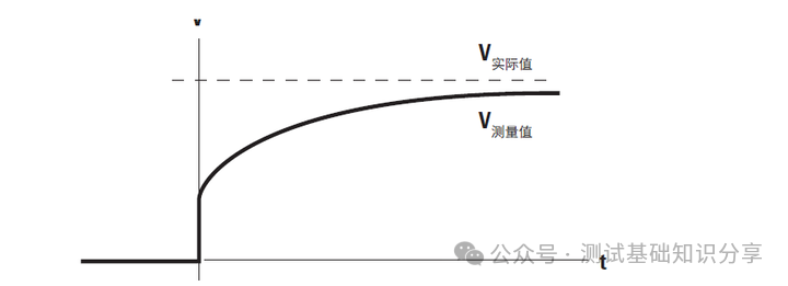
Figure 3. Capacitive load alters the measured signal waveform by inducing exponential responses.
Figure 4 shows the input impedance of oscilloscope probes up to 6 GHz. You can see that at low frequencies below 1 MHz, the probe input impedance is primarily determined by the probe’s DC resistance component (100 kΩ). As the signal frequency increases, capacitive reactance gradually becomes the main component affecting circuit load. At 2 GHz, the impedance of the oscilloscope probe reaches its lowest level of 165 Ω, determined by the probe resistor.
We can use a digital signal with ultra-fast edges generated by a 25 Ω signal source (see Figure 5) to illustrate how these probe factors affect the measured waveform and the circuit under test. You can see that when the probe connects to the circuit under test, the signal waveform changes due to the probe input impedance.
Inductive load appears in the measured signal as ringing (see Figure 6). The signal source generating the ringing is an LC circuit, composed of the internal capacitance of the probe and the inductance of the ground lead and probe. When performing any type of oscilloscope measurement, it is advisable to use the shortest possible ground lead. This can reduce inductance and shift the ringing frequency outside the bandwidth of the oscilloscope and probe, thereby minimizing its impact on the measurement.
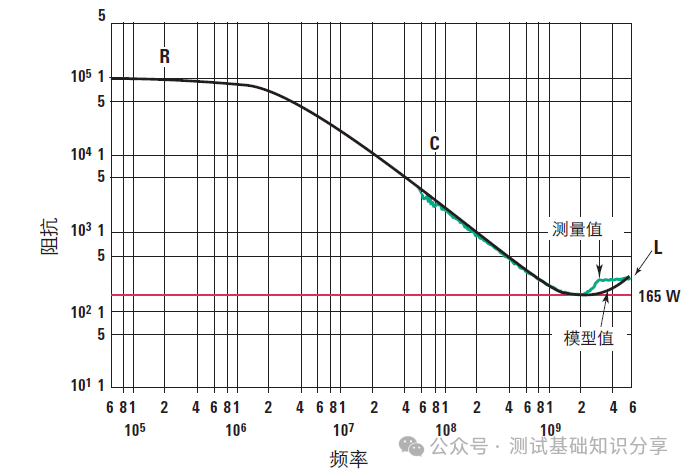
Figure 4. Increasing frequency can change the input impedance of the oscilloscope probe.
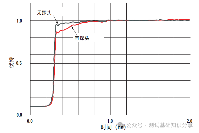
Figure 5. The oscilloscope probe causes circuit loading under high-frequency conditions and extends the time for the circuit to produce full voltage.
What is the transmission response of an oscilloscope probe?
The parasitic parameters that affect the input impedance of the oscilloscope probe and cause changes in the probe’s transmission response are commonly referred to as the probe transmission response. This transmission response is defined as the ratio of the probe output voltage to the probe input voltage (Vout/Vin), typically displayed as an amplitude (dB) vs. frequency graph.
When the transmission response is below -3 dB or the amplitude drops to 70.7%, the probe bandwidth is the continuous frequency range (Figure -6). At frequencies outside the probe bandwidth, the signal amplitude will be excessively attenuated, making measurement results unpredictable.
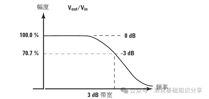
Figure 6. Bandwidth refers to the continuous frequency range when the instrument’s transmission response drops by 3 dB.
Within the probe bandwidth, you can see that the probe output signal closely matches the probe input signal, with minimal deviation, so the waveform you see on the oscilloscope screen is the signal at the probe input.
In the frequency domain, the probe’s ability to transmit signals from input to output while minimizing its impact on the signal is reflected in a very flat transmission response (0 dB) across the entire probe bandwidth. However, achieving this in practical conditions is challenging. When the probe connects to the circuit under test, the parasitic effects of the physical connection and the internal components of the probe can form a resonant circuit, with a resonant frequency below the probe bandwidth (Figure 7). This in-band resonance will cause discrepancies between the probe output signal and the input signal, manifesting as overshoot and ringing in the measured waveform.
Figure 7 illustrates the in-band impedance on the input voltage (Vin) of a 4-GHz probe from Tektronix. Note that at this time, the probe output voltage (Vout) does not match the input voltage. The output voltage remains flat, while the probe transmission response (Vout/Vin) peaks at 5 dB.
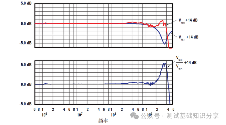
Figure 7. (Top) Frequency response of the input voltage and output voltage of Tektronix’s 4 GHz probe in a 25-Ω system. (Bottom) The probe’s transmission response. When the input voltage resonates down to 3.5 GHz, the output voltage remains flat, and the transmission response peaks at 5 dB.
So what is the issue when the input voltage resonates while the output voltage remains flat? Isn’t this the same as the signal situation when the probe is not connected? This is a good question, but remember that the probe transmission response will always be at a peak of 5 dB, leading to distortion of the input signal and displaying additional overshoot and ringing in the measured waveform.
Figure 8 shows measurements taken at the midpoint of a transmission line terminated with a 50-Ω load, with the signal source resistance shown as 25 Ω, and the probe response matches this type of circuit. If the circuit being measured cannot provide an ideal 25-Ω signal source resistance, you will see signal distortion caused by the probe.
We can better explain this type of distortion through an example. Suppose you use a 100-kΩ probe to measure the voltage of a circuit with a 100-kΩ signal source resistance, and the transmission response of that probe has been modified for this type of circuit, it can display the probe’s “actual” output voltage. Therefore, when you connect the probe to the circuit and reduce the input voltage by half, the measured waveform will display the full voltage amplitude as if the probe were not connected.
However, what happens when the probe connects to a circuit with a 50-kΩ signal source resistance? The probe’s transmission response will still alter the measured waveform, displaying a waveform voltage that is 33% higher than the actual voltage at the probe input.
The best oscilloscope probes can ensure minimal impact on the circuit under test and the least voltage distortion from input to output. This way, you can observe the signal at the probe.
Oscilloscope probes can address such issues by installing a resistor close to the measurement point. Installing a resistor on the probe can isolate the parasitic effects of the probe on the circuit under test and suppress the formation of resonant circuits. This can keep the probe transmission response (Vout/Vin) flat across the entire bandwidth up to 4 GHz (Figure 8).
Typically, if precise rise time measurements are required, the shortest possible ground leads should be used.
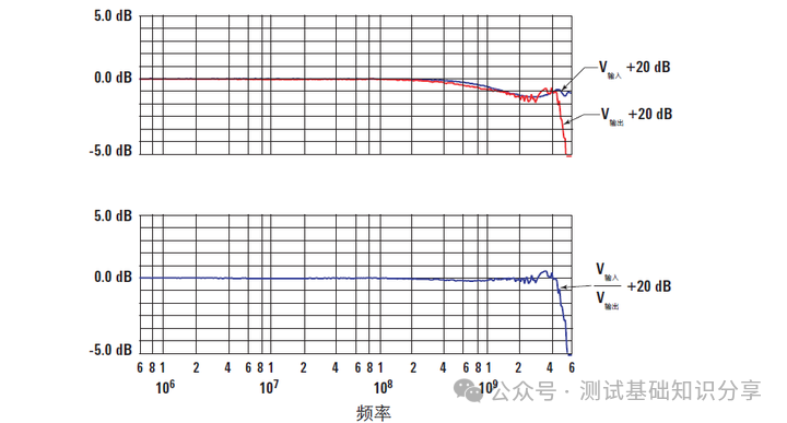
Figure 8. (Top) Frequency response of the input voltage and output voltage of the oscilloscope probe. (Bottom) Although the frequency response of the output voltage closely matches the input voltage, the probe transmission response remains flat across the entire 4 GHz bandwidth.
Oscilloscope probe accessories
Due to the challenges in probing circuits, it is not always possible to connect the probe directly to the signal and ground. Therefore, we often see a small piece of wire soldered onto the circuit to facilitate the probe’s connection to the signal and ground. However, these wires can introduce more parasitic effects, significantly altering the probe’s transmission response, leading to overshoot and ringing in the measured waveform (Figure -9). Typically, when using wires to extend the probe’s detection range, each inch of wire can introduce up to 25 nH of inductance into the probe’s equivalent circuit.
How to test signals on the circuit board that the probe cannot detect?
So how do we test those signals on the circuit board that the probe cannot detect?
Most high-performance probes provide attachments that allow for physical connections but do not have electrical characteristics suitable for transmitting high-fidelity signals.
Oscilloscope probes and their accessories form a complementary and indispensable measurement system. Various accessories for oscilloscope probes help you achieve these challenging connections and optimize measurement performance through appropriately controlled electrical characteristics.
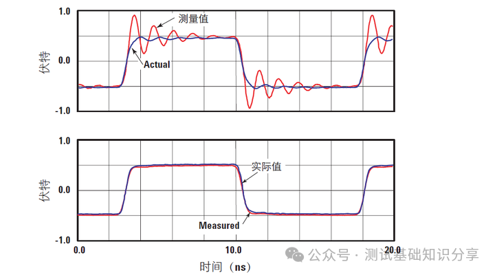
Figure 9. Measurements on a 66 MHz/500-ps clock. (Top) A standard 5-cm wire connected to the measured signal causes overshoot and ringing in the measured waveform. (Bottom) A properly damped 5-cm resistive signal wire helps the probe access tight spaces for detection without distorting the measured waveform.
Probe accessories
Oscilloscope probes typically offer 5-cm and 10-cm resistive signal leads to assist the probe in detecting in tight spaces (Figure -10). These signal leads include resistive probes that can isolate the probe’s parasitic effects from the circuit under test and suppress the formation of resonant circuits.
This allows for a flat transmission response across the entire bandwidth of the detection system (Figure 11). Ultimately, you can measure signals at hard-to-reach measurement points without introducing additional overshoot, ringing, or other distortions into the measured waveform!
Remember, it is essential to use the shortest possible ground leads.When the ground lead connects to the probe, inductance is introduced into the probe return path, which cannot be compensated for in the probe. Additional inductance will alter the probe’s transmission response and lead to distortion in the measured waveform.
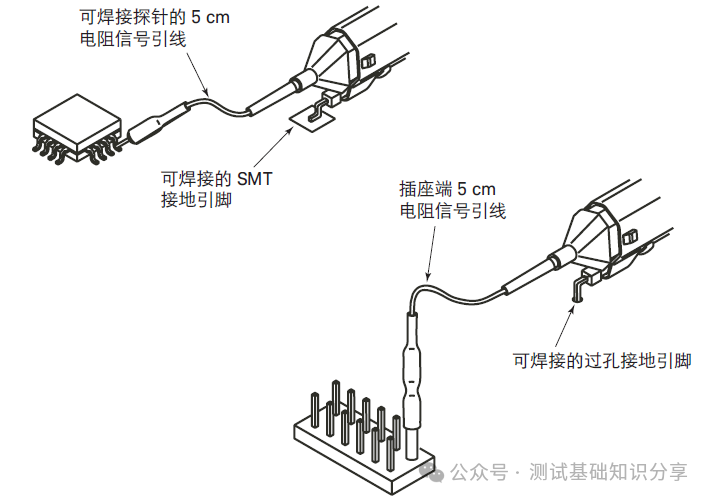
Figure 10. Probing with an oscilloscope probe and properly damping the accessories to improve measurement reliability.
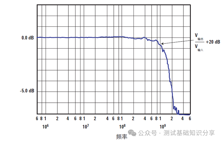
Figure 11. Although probing with a 5 cm resistive signal lead reduces measurement bandwidth, the transmission response remains flat and does not introduce distortion into the measured waveform.
Bandwidth and Rise Time Considerations
When selecting an oscilloscope and probe, it is essential to understand the bandwidth limits, as they can affect measurement accuracy. Bandwidth refers to the frequency at which the measurement system’s transmission response causes the output voltage amplitude to drop from the reference level by -3 dB (70.7%) (Figure -6). So what bandwidth do your oscilloscope and probe need?
Signals transmitted by continuous sine waves consist of a single frequency component, the fundamental frequency. The closer the sine wave frequency is to the bandwidth limit of the measurement system, the more the measurement amplitude will attenuate. Within the system bandwidth, it is expected that the amplitude of the measured sine wave will have a 30% error. Therefore, for precise amplitude measurements, you should choose an oscilloscope and probe with a fundamental bandwidth three times that of the signal’s fundamental frequency.
Unlike sine signals that contain only a single frequency component, digital signals encompass a wide spectrum of frequency components at multiple frequencies to form square waves with fast edge speeds. The spectral content of digital signals is primarily determined by edge speed rather than the signal repetition rate. A conservative estimate for the edge frequency of digital signals is:
F = 0.5/(rise time)
Typically, the estimated frequency is slightly higher than the actual frequency.
Digital signals also have significant third and fifth harmonic frequency components. The attenuation of these high-frequency components will cause rise time and fall time measurements to be slower than the actual times. Therefore, to improve the accuracy of rise time and fall time measurements, you should choose an oscilloscope and probe with a bandwidth three or five times the rise time frequency of the digital signal.
How to determine the system bandwidth of the oscilloscope and probe?
Now that we know the bandwidth requirements for accurately capturing signals, how do we determine the system bandwidth of the oscilloscope and probe?
All types of probes have bandwidth limit values, so there is a minimum signal rise time that can be achieved through the probe, which can be calculated using the following formula:
Rise time = 0.35/bandwidth
Rise time refers to the time required for the waveform to transition from 10% to 90% of its final value. The shortest rise time and fall time of the probe (detailed in the probe specifications) indicate the rise time and fall time of the probe output signal when the input signal is a step signal with a rise time of zero. This can be observed by examining the input and output signals of the oscilloscope probe (Figure 12).
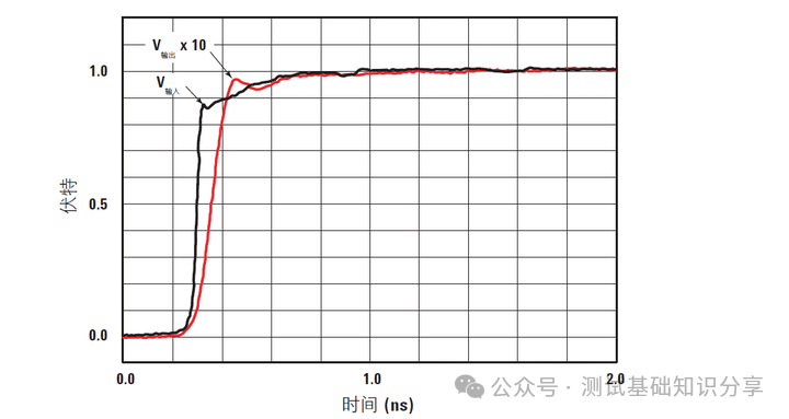
Figure 12. The shortest rise time of the probe affects measurement results.
Oscilloscope Bandwidth and Rise Time
Oscilloscopes also have independent bandwidth and rise time limit values. It is generally believed that the bandwidth of the oscilloscope and probe should be equal. However, the relationship between oscilloscope bandwidth and probe bandwidth is not that simple.
The oscilloscope and probe form a measurement system, and the transmission response of this system will include both the probe transmission response and the oscilloscope transmission response. These combined responses will determine the rise time and bandwidth of the measurement system, which can typically be calculated using the following formula:

These formulas apply to calculating the system bandwidth and rise time of the oscilloscope and probe response when the response decays according to Gaussian law (Figure 13).
If the response does not conform to Gaussian law, you must take a closer look at the probe response to understand how the signal is transmitted from the probe to the oscilloscope input. As long as the probe response is flat, i.e., Vout/Vin = 0 dB, the signal transmitted to the oscilloscope input will be identical to the probe input signal.

Figure 13. Comparison of Gaussian transmission response and rapid decay response of the oscilloscope probe.
Bandwidth and Rise Time Considerations
Tektronix adheres to the principle of achieving maximum response flatness in developing the 1156A/57A/58A probes. Figure -14 shows the transmission response of these probes.
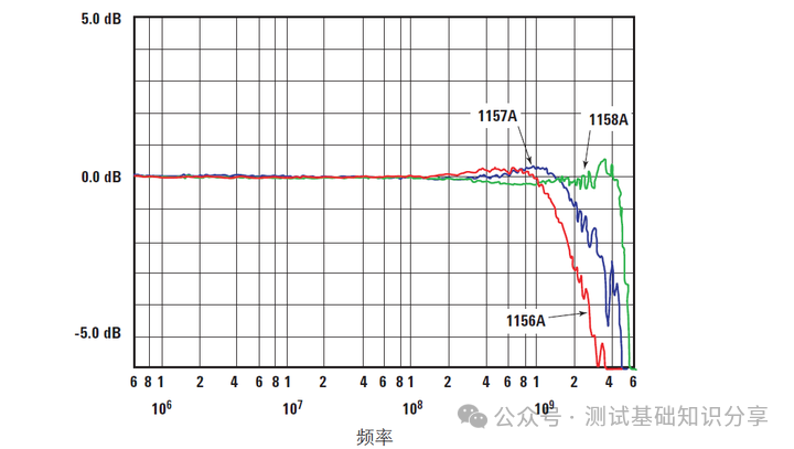
Figure 14. Transmission response of oscilloscope probes.
Conclusion
As the frequency of electronic devices continues to rise, selecting the appropriate oscilloscope probe becomes a key factor in determining measurement results and the operation of the circuit under test.
When selecting a new probe, consider the following factors:
-
Check the input impedance of the oscilloscope probe and consider its impact on the circuit. At high frequencies, the load has an increasingly significant effect, so be sure to use the shortest possible ground leads.
-
The oscilloscope probe should have a flat transmission response across its entire bandwidth, otherwise, it will cause measurement result distortion. A flat transmission response ensures that the probe output signal matches the probe input signal perfectly and transmits it intact to the oscilloscope.
-
The best measurement results depend on the oscilloscope probe and connections, so wisely choosing and properly using probe damping accessories can improve the accuracy and repeatability of measurement results.
-
The oscilloscope and probe work together to form a complete measurement system. Fully understanding the impact of the probe on the overall system bandwidth can help you confidently select the oscilloscope and probe that best suit your application.
The best probes can ensure minimal impact on the circuit under test and the least voltage distortion from input to output.The best oscilloscope probescan ensure minimal impact on the circuit under test and the least voltage distortion from input to output.Oscilloscope probesprovide leading performance, enabling the most accurate analysis of high-speed circuits.
Do not forward without permission.