[OSP (Organic Solderability Preservative) is a chemical method that grows a layer of organic copper complex compound on the surface of copper. This organic film can protect the clean bare copper on the circuit board from rusting (sulfidation or oxidation) in normal storage environments by preventing contact with air, and it can be easily removed during the PCB assembly process by flux and dilute acid, exposing the clean copper surface for soldering with molten solder.
This OSP is essentially a transparent protective film, which is generally difficult to detect with the naked eye. Experts can determine whether there is a transparent film on the copper foil by observing the refraction of light. Since OSP-treated boards do not visually differ much from regular bare copper boards, this also complicates the inspection and measurement processes in board manufacturing.
If there are holes in the organic copper preservative (OSP) directly on the copper surface, oxidation will begin at the holes, adversely affecting SMT assembly. The thicker the organic copper preservative, the better the protection for the copper foil, but it also requires a more active flux to remove it for soldering. Therefore, the thickness of the OSP film is generally required to be between 0.2-0.5um.
Production Flowchart of OSP (Organic Solderability Preservative)
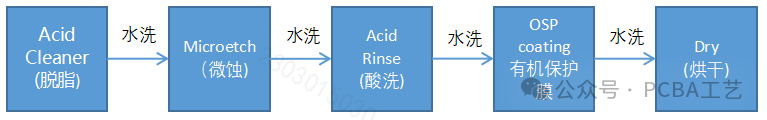
Acid Cleaner (Degreasing):
The main purpose is to remove any copper surface oxides, fingerprints, and grease that may have occurred during the previous processes to achieve a clean copper surface.
Micro-etch (Micro-etching):
The main purpose of micro-etching is to remove more severe oxides from the copper surface and to create a uniformly bright micro-rough copper surface, allowing the subsequent OSP film to adhere more finely and evenly. Generally, the gloss and color of the copper surface after OSP film formation are positively correlated with the micro-etching solution used, as different solutions can cause different roughness on the copper surface, which affects the refraction rate and angle of light.
Acid Rinse (Acid Washing):
The function of acid washing is to thoroughly remove any residual substances on the copper surface after micro-etching, ensuring the copper surface is clean for the next process.
OSP Coating (Organic Solderability Preservative Treatment):
A layer of organic copper complex compound is grown on the copper surface to protect it from oxidation during storage. The thickness of the OSP film is generally required to be between 0.2-0.5um.
Factors affecting OSP film formation include:
pH value of the OSP bath solution
Concentration of the OSP bath solution
Total acidity of the OSP bath solution
Operating temperature
Reaction time
After OSP, the water rinse should strictly control the pH value above 2.1 to avoid overly acidic rinsing that could erode the OSP film, resulting in insufficient thickness.
Dry (Drying):
To ensure that the coating layer on the board surface and inside the holes is dry, it is recommended to use hot air at 60-90°C for 30 seconds. (This temperature and time may vary depending on the OSP material used.)
Advantages of OSP (Organic Solderability Preservative) Surface Treatment for PCBs:
1.Cost-effective.
2.Excellent soldering strength; the soldering strength of OSP copper base is generally better than that of ENIG nickel base.
3.Expired (three or six months) boards can be reprocessed, but usually only once, depending on the condition of the board.
Disadvantages of OSP (Organic Solderability Preservative) Surface Treatment for PCBs:
1.OSP is a transparent film, making it difficult to measure its thickness, thus hard to control. If the film is too thin, it fails to protect the copper surface; if too thick, it hinders soldering.
2.For secondary reflow soldering, it is recommended to operate in a nitrogen environment to achieve better soldering results.
3.Shelf life is relatively short. Generally, OSP has a maximum shelf life of six months after completion at the board factory, with some only lasting three months, depending on the factory’s capabilities and the quality of the board. Some boards exceeding the shelf life can be sent back to the factory to remove the old OSP from the PCB surface and apply a new layer. However, removing the old OSP film requires corrosive chemicals, which may corrode the original copper surface, potentially damaging it. If the pads are too small, they cannot be processed, and communication with the factory is necessary to determine if reprocessing is possible.
4.Susceptible to acid and humidity. When used for secondary reflow soldering, it must be completed within a certain time; typically, the results of the second reflow soldering are poorer. It is generally required to be used within 24 hours after opening the package (after reflow). The shorter the time between the first and second soldering, the better; it is generally recommended to complete the second soldering within 8 to 12 hours.
OSP is an insulating layer, so test points on the board must be printed with solder paste to remove the original OSP layer to make contact for electrical testing.
5.OSP boards are copper-based, and initially, soldering will generate a benign Cu6Sn5 intermetallic compound (IMC), but over time, it will gradually change to a detrimental Cu3Sn IMC, affecting reliability. Therefore, if long-term use in high-temperature environments or products requiring a longer lifespan is needed, the long-term reliability of OSP must be carefully considered.
Personal Opinion on OSP Surface Treatment for PCBs:
The above information can be found online regarding OSP boards, but there are many issues to pay attention to in actual production processes. For example, whether our board process includes wave soldering, because if the SMT process is completed and it is an OSP board, the time for the product to transition from SMT to through-hole production (generally required to be 24H) must be strictly controlled. Otherwise, once the copper foil in the through holes oxidizes, various issues such as insufficient solder, solder voids, and other problems become unavoidable. Additionally, as previously mentioned, test points must be soldered; otherwise, it may affect the test pass rate. Another point is that OSP boards are generally required not to expose copper after completing SMT, as the copper foil without the organic protective film is prone to oxidation. If there is no solder coverage, the exposed copper will oxidize upon contact with moisture in the air, leading to corrosion over time, significantly reducing the lifespan of the PCBA. Therefore, certain areas, such as chip grounding pads and screw holes, must be soldered.
If you find this helpful, please like, save, and follow. This is my motivation for updates.886.