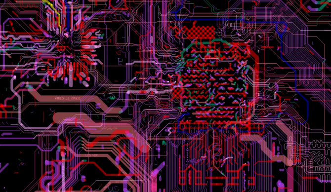
When hardware engineers first encounter multi-layer PCBs, it can be quite overwhelming. With sometimes ten or more layers, the layout resembles a spider web. Are you still struggling?
Today, I’ve created several internal structure diagrams of multi-layer PCBs, using 3D graphics to display various stacking structures of PCB internal architecture, helping you to see clearly.
The Core of High-Density Interconnect Boards (HDI) is the Via
The processing of multi-layer PCB traces is not much different from single or double-layer boards; the biggest difference lies in the via technology.
Traces are etched, while vias are drilled and then copper-plated, which everyone involved in hardware development understands, so I won’t elaborate further.
Multi-layer circuit boards typically include through-hole boards, first-order boards, second-order boards, and second-order stacked via boards. Higher-order types, such as third-order boards and arbitrary-layer interconnect boards, are rarely used due to their exorbitant prices, so I won’t discuss them further.
Generally, 8-bit microcontroller products use 2-layer through-hole boards; 32-bit microcontroller-level smart hardware uses 4 to 6 layers of through-hole boards; Linux and Android-level smart hardware uses 6 layers of through-hole to 8 first-order HDI boards; compact products like smartphones typically use 8 to 10 layers of second-order circuit boards.
8-layer second-order via, Qualcomm Snapdragon 624
The Most Common Through-Hole
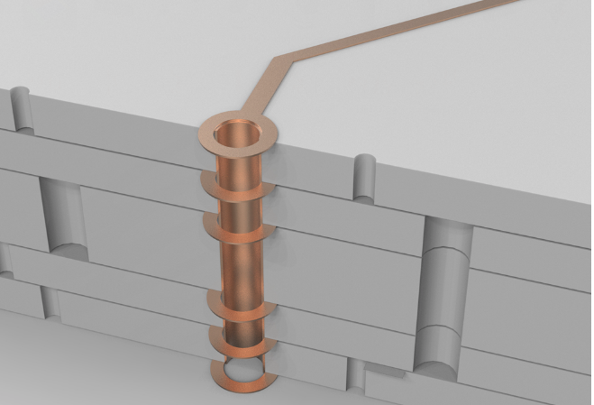
There is only one type of via, from the first layer to the last layer. Regardless of whether the traces are external or internal, the holes are drilled through, known as a through-hole board.
Through-hole boards are unrelated to the number of layers; commonly used 2-layer boards are through-hole boards, while many switches and military circuit boards can have 20 layers and still be through-hole.
Using a drill bit to penetrate the circuit board, copper is plated into the holes to form a connection.
It is important to note that the inner diameters of through-holes typically are 0.2mm, 0.25mm, and 0.3mm, but generally, 0.2mm is significantly more expensive than 0.3mm. This is because thinner drill bits are more prone to breaking and take longer to drill. The additional time and cost of the drill bits reflect in the increased price of the circuit board.
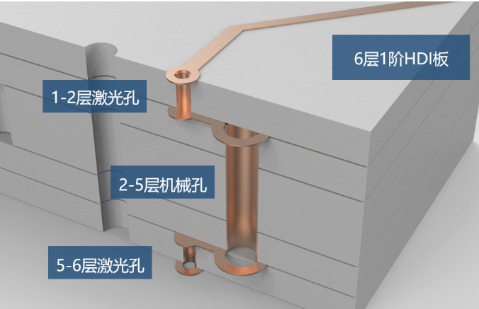
Laser Vias in High-Density Boards (HDI Boards)
This image shows the stacking structure of a 6-layer first-order HDI board, with the outer two layers featuring laser vias with a 0.1mm inner diameter. The inner layers are mechanical vias, equivalent to a 4-layer through-hole board covered by an additional 2 layers.
Lasers can only penetrate glass fiber materials and cannot penetrate metal copper. Therefore, drilling holes on the outer surface does not affect other internal traces.
After the laser drills the holes, copper is plated to form laser vias.
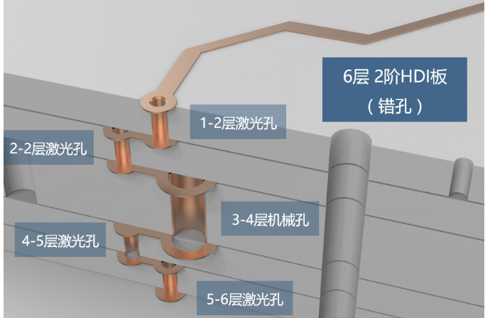
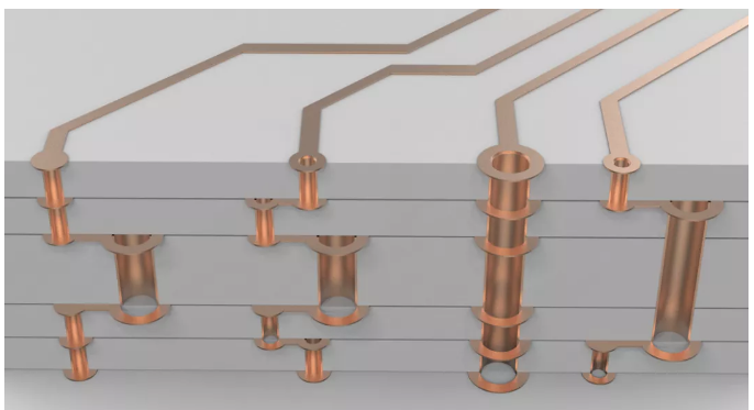
Second-Order HDI Board with Two Layers of Laser Vias
This image shows a 6-layer second-order staggered via HDI board. Generally, second-order 6-layer boards are less common, with most starting from 8 layers. The additional layers follow the same principle as the 6-layer boards.
Second-order means there are two layers of laser vias.
Staggered vias mean the two layers of laser vias are offset.
Why offset? Because copper plating cannot fill completely, leaving the holes empty, so you cannot drill directly on top; you must offset a certain distance before drilling another layer.
A 6-layer second-order board = a 4-layer first-order board plus 2 layers.
An 8-layer second-order board = a 6-layer first-order board plus 2 layers.
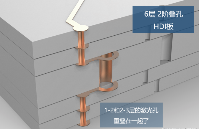
Stacked Via Boards: Complex Process, Higher Cost
In staggered via boards, the two layers of laser vias overlap. The traces become more compact.
The inner laser vias need to be plated flat before making the outer laser vias. This process is slightly more expensive than staggered vias.
Extremely Expensive Arbitrary Layer Interconnect Boards with Multi-layer Laser Vias
Every layer features laser vias that can connect to each other. You can route traces and drill holes as you wish.
Layout engineers must feel great just thinking about it! No more worries about not being able to design it!
Procurement managers might cry just thinking about it, as they cost over ten times more than regular through-hole boards!
Thus, only products like the iPhone can afford to use them. Other smartphone brands have not been reported to use arbitrary layer interconnect boards.
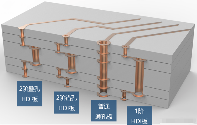
Finally, here’s a picture for a detailed comparison.
Please pay attention to the size of the holes and whether the pads are closed or open.
———— / END / ————
Source: “Electronic Engineering Magazine”
Intelligent Manufacturing