The edges of printed circuit boards include the outer edge, the inner milled edge, and the edge of non-plated holes, which are one of the items for visual inspection. Common defects include burr, nick, haloing, crazing, delamination, and blister.
Burr: Irregular protrusions or edges on the edges of printed boards caused by processes such as drilling, milling, or depaneling, classified into metal burrs and non-metal burrs.

Figure 1: Burrs on the edges of printed circuit boards
Nick: Local material loss and damage on the edges of printed boards caused by processes such as drilling, milling, or depaneling.
Haloing: Ring-shaped or foggy discoloration areas appearing on the edges of printed circuit boards, usually manifested as a lightening, whitening, or translucent appearance of the substrate color.
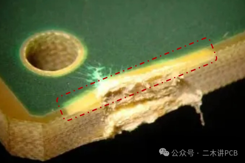
Figure 2: Haloing on the edges of printed circuit boards
Crazing: Refers to linear cracks appearing on the edges of printed circuit boards due to thermal or mechanical stress, usually extending along the fiber direction of the substrate, potentially penetrating the surface layer or deeply into the internal multilayer structure.
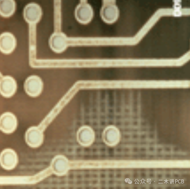
Figure 3: Cracks on the edges of printed circuit boards
Delamination: Refers to the failure of bonding strength between layers of the substrate at the edges of printed circuit boards, forming visible gaps to the naked eye or under a microscope.
Blister: Refers to visible raised bubbles between the substrate or copper foil and the substrate on the edges of printed circuit boards.
Standards: IPC-6012F “Qualification and Performance Specification for Rigid Printed Boards”, GJB 362C “General Specification for Rigid Printed Boards”, GJB 9491 “General Specification for Microwave Printed Boards”, and other standards specify the requirements for burrs on the edges of printed circuit boards. It is recommended that the inspection process be qualified according to the following items:
1. The edges of the substrate are cut neatly, smooth, and free of metal burrs (for non-metal edged printed circuit boards);
2. Non-metal burrs are acceptable as long as they are not loose and do not affect assembly and functionality;
3. The total length of nicks and cracks extending inward from the edge should not exceed 50% of the distance from the board edge to the nearest conductive pattern or 2.5mm, whichever is smaller;
4. Delamination, haloing, and blistering should be at least the minimum spacing requirement specified for adjacent conductive patterns in the layout plan. If not specified, it should be no less than 0.1mm.
5. For printed circuit boards with metal edges (metalized edges), separation of the edge metal from the dielectric is allowed, but separation from conductors interconnecting the inner layers is not allowed. The number of voids in the side metal plating should not exceed 3, and any length should not exceed 1.27mm. Protrusions of the side metal are acceptable as long as they are not loose and do not violate the overall size requirements of the printed circuit board. After depaneling, exposed copper at the breakaway tab position is acceptable, provided that the metal burrs are not loose and do not affect assembly and functionality.