The eight major process systems of PCBA (Printed Circuit Board Assembly) cover the entire process from component placement to finished product testing and packaging, detailed as follows:
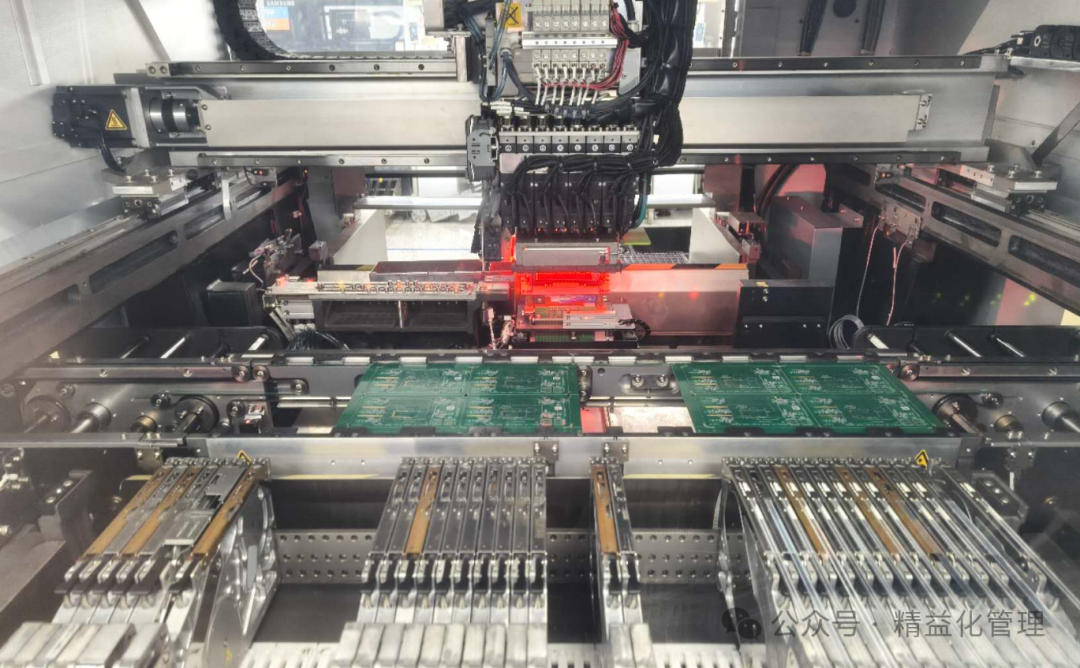
1. SMT (Surface Mount Technology) Process
Process: Solder paste printing → Component placement → Reflow soldering
Function: Precisely place surface mount devices (SMD) onto PCB pads and form reliable connections through high-temperature reflow soldering.
Key Equipment: Solder paste printer, pick-and-place machine, reflow oven.
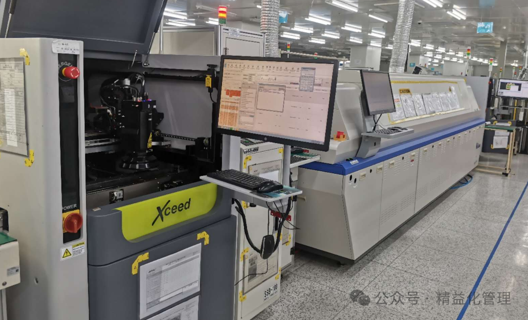
2. Reflow Soldering Process
Process: Preheating → Constant temperature → Reflow → Cooling
Function: Melt solder paste through precise temperature control to achieve electrical and mechanical connections between SMD and PCB.
Characteristics: Suitable for high-density, miniaturized components, with good soldering consistency.
3. THT (Through-Hole Technology) Process
Process: Insertion → Wave soldering/manual soldering
Function: Insert through-hole components (such as connectors, electrolytic capacitors) into PCB holes and secure them through wave soldering or manual soldering.
Key Equipment: Insertion line, wave soldering machine, manual soldering station.
4. Wave Soldering Process
Process: Preheating → Flux spraying → Wave soldering → Cooling
Function: Utilize molten solder wave to complete the soldering of through-hole components in one go.
Applicable Scenarios: Soldering of large quantities of simple structure through-hole components.
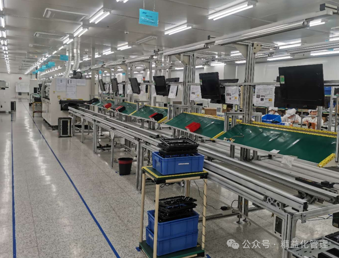
5. Inspection and Quality Control Process
Technical Means:
AOI (Automated Optical Inspection): Check for appearance defects in solder joints (such as cold solder, misalignment).
X-Ray Inspection: Inspect the quality of hidden solder joints such as BGA and QFN.
ICT (In-Circuit Testing): Verify circuit connectivity and component parameters.
Goal: Ensure that soldering quality and electrical performance meet standards.
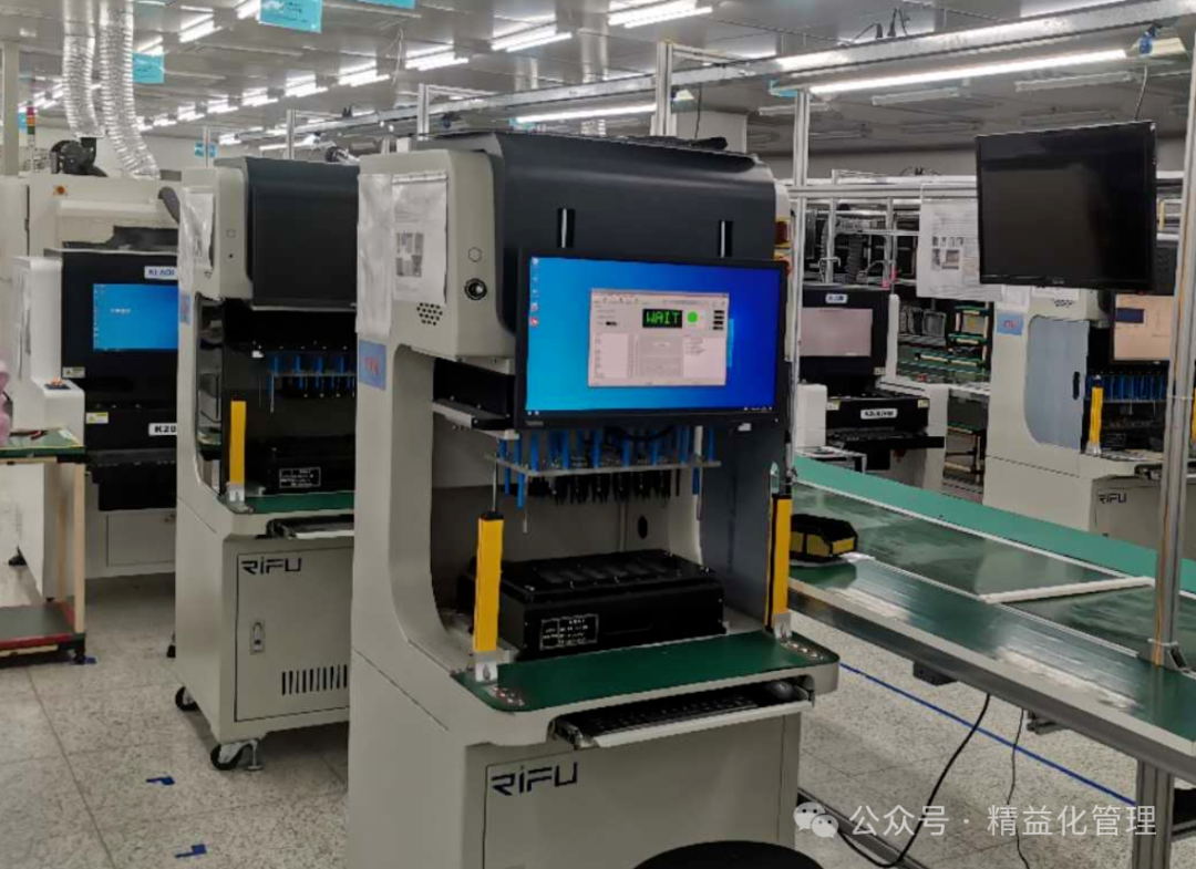
6. Functional Testing (FCT, ATE) Process
Process: Simulate real working environment → Test overall board functionality → Fault diagnosis
Function: Verify whether the PCBA meets design functions, such as signal integrity, power consumption, communication protocols, etc.
Tools: Custom test fixtures, automated testing software.
7. Cleaning and Protection Process
Cleaning: Use deionized water or solvents to remove flux residues to prevent corrosion or short circuits.
Conformal Coating: Spray moisture-proof, mildew-proof, and salt spray-proof coatings to enhance product environmental adaptability.
Application Scenarios: Automotive electronics, industrial equipment, and other harsh environments.
8. Assembly and Packaging Process
Assembly: Integrate PCBA with enclosures, heat sinks, and other structural components into a complete product.
Packaging: Anti-static and shock-proof packaging to ensure safe transportation.
Standards: Follow ESD protection and customer customization requirements.
Summary
The eight major process systems are interconnected, covering the entire chain from placement, soldering, inspection to finished products. Quality control at each step directly affects the reliability and performance of the final product. With the development of technology, automation (such as intelligent AOI, FCT, ATE) and environmentally friendly processes (such as no-clean solder paste) have become industry trends.