
Source: Chip Forum
Author: Tian Gao Yun Dan Andi863
Introduction: The author attempts to introduce chip manufacturing in the simplest and most popular language. If professionals find inaccuracies, please feel free to provide feedback. I wanted to keep it shorter and simpler, but due to the complexity and specialization of chip manufacturing, this article may still seem lengthy. I appreciate your understanding!
Chip manufacturing is the second specialized link in the chip industry chain.The core value of chip manufacturing plants is to standardize, mature, and platformize their specialized chip manufacturing processes, specifically undertaking commissioned processing of corresponding types of chips from chip design companies, providing professional chip manufacturing services for clients. Chip manufacturing plants are also known as foundries.
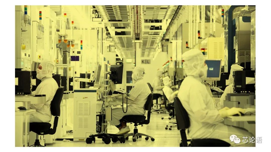
Figure 1. Factors in chip manufacturing: Equipment (capital investment),
Talent (management level), Process (technical accumulation)
The professional indicators of chip manufacturing plants mainly include:Wafer materials (gallium arsenide, silicon, silicon carbide, gallium nitride, etc.), wafer sizes (4 inches, 8 inches, 12 inches, etc.), process types (analog, digital, high voltage, memory, MEMS, etc.), feature line widths (…28nm, 14nm, 7nm, 4nm, etc.), process yield, and delivery times. These indicators are essential for chip design companies to understand and be familiar with. Generally, a chip design project targets a specific process at a certain foundry. In special cases, if the target process needs to be transferred, the backend design of the chip needs to start over.
The most ingenious technology in chip manufacturing is planar processing technology.Planar processing technology involves processing the entire surface of the wafer layer by layer, stacking to form all the transistors and circuit connections on all chips on the wafer. For example, Huawei’s Kirin 990 5G chip has an area of 113 square millimeters, and approximately 600 chips can be arranged on one wafer, with each chip containing 10.3 billion transistors and circuit connections. After completing the planar processing flow, all 600 chips on the wafer are simultaneously manufactured. Planar processing is fundamentally different from traditional product processing (processing products one by one). It is akin to printing text on paper, where printing is a planar processing technology, while typing is traditional processing technology.
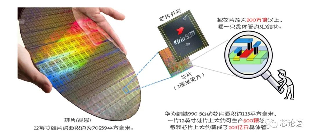
Figure 2. Planar processing technology processes the entire wafer,
simultaneously obtaining numerous chips
Cooking relies on frying, stir-frying, and boiling,while chip manufacturing primarily relies on the three main techniques of planar processing technology: “doping,” “growth,” and “etching.” “Doping” refers to incorporating specific impurity elements into the semiconductor substrate material to alter its local conductivity. “Doping” can be divided into diffusion and ion implantation. “Growth” refers to growing a layer of semiconductor material or dielectric thin film (e.g., oxide layer, polysilicon, metal interconnect layer, etc.) on the underlying material, with “growth” divided into oxidation, chemical vapor deposition, and metalization. “Etching” refers to removing unnecessary parts from the dielectric thin film according to the chip design pattern, leaving the useful parts. “Etching” is divided into photolithography and etching stages. Photolithography is used to transfer the chip design pattern onto the photoresist layer on the dielectric thin film, while etching removes the parts of the dielectric thin film that are not protected by the photoresist pattern. Photolithography is also used to define the diffusion or ion implantation areas for “doping.”
The seven chip manufacturing processes described above are briefly outlined as follows: 1. Oxidation is generating a layer of oxide film in a specified area. 2. Diffusion is quantitatively incorporating other elements’ atoms into a specified area, altering the electrical properties of that area. 3. Ion implantation is quantitatively injecting impurity elements’ atoms or particles into a specified area to change its electrical properties. Compared to diffusion, ion implantation has no overflow effect, and its depth and dosage are easily controlled. 4. CVD/PVD is depositing a layer of silicon oxide, silicon carbide, polysilicon, etc., in a specified area. 5. Metalization is depositing a metal thin layer on the insulating dielectric thin film, forming metal interconnects and vias through photolithography and etching. 6. Photolithography utilizes exposure and development to accurately replicate the geometric pattern on the mask onto the photoresist layer. 7. Etching is removing parts of the dielectric thin film that are not protected by the photoresist pattern using chemical or physical methods. Combining photolithography and etching allows for accurately replicating the mask pattern on semiconductor materials. Due to space limitations, many complementary manufacturing processes (such as polishing, cleaning, sputtering, planarization, passivation, electroplating, etc.) will not be introduced in this article.
Taking the CMOS chip manufacturing process as an example to introduce the chip manufacturing process.The chip manufacturing process involves the repeated use of the main manufacturing processes mentioned above. First, the chip layout (design) is made into a set of multiple photomasks in a certain order (as shown in Figure 3). Second, according to the corresponding photomask pattern, “doping” is performed on the wafer substrate to alter the semiconductor conductivity in certain areas. Next, layers of patterned dielectric thin films (including oxide layer, polysilicon gate layer, passivation layer, metal interconnect layer, etc.) are created on the wafer substrate according to the photomask pattern. For each layer, the dielectric thin film is “grown” on the underlying layer, then the photomask pattern is transferred to this dielectric thin film using photolithography, followed by “etching” to create the pattern of this material layer. The layered patterned dielectric thin films (with specific thicknesses, see the diagram below c) are stacked on the wafer substrate according to the chip design requirements, constituting all transistors and interconnections of all chips on the wafer. After completing all the process steps of planar processing on the wafer, all chips will be simultaneously manufactured, awaiting subsequent cutting, packaging, and testing.
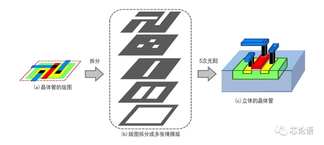
Figure 3. Chip layout, photomask, and the stacking of dielectric thin films on the chip
to form a circuit diagram (part of the chip, structure of a transistor)
Currently, only TSMC, Samsung, and Intel are competing in the global market for wafer foundries at 10nm and more advanced chip processes. TSMC and Samsung are in competition at 7nm, 5nm, and even 3nm, while China’s largest and most advanced foundry, SMIC, has achieved breakthroughs in 14nm technology.
How precise are advanced chip manufacturing processes? Taking the 7nm process as an example, it can create over 6000 circuit connections on a silicon wafer the size of a hair’s cross-section, and integrate over 100 million transistors and their circuit connections on a square millimeter silicon wafer (half the size of a sesame seed).
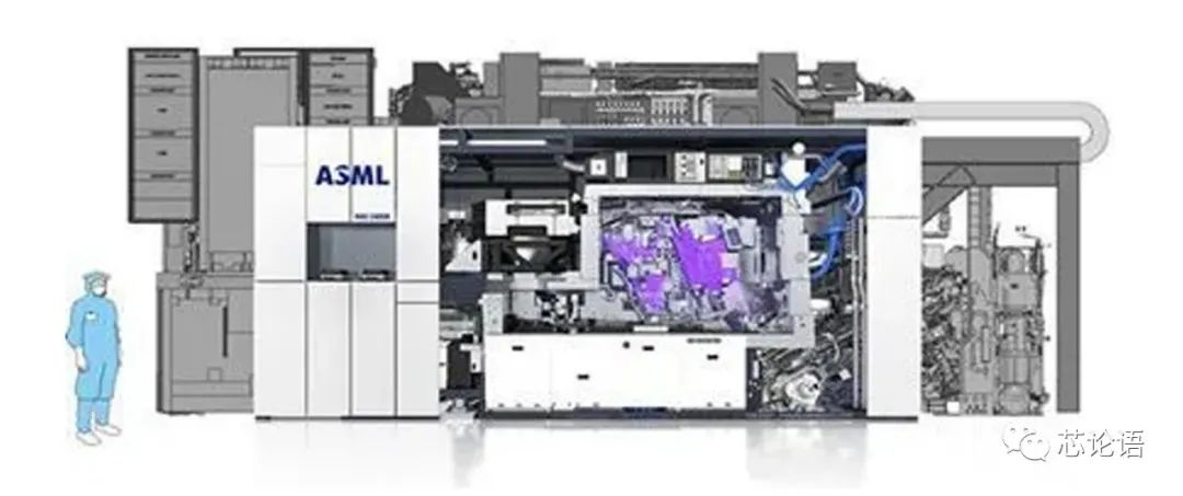
Figure 4. A $120 million EUV lithography machine
Advanced and precise chip manufacturing requires even more sophisticated manufacturing equipment. For instance, each EUV lithography machine, valued at over $120 million, is essential for 7nm and more advanced process technologies. Advanced foundries require massive capital investments each year; for instance, the three major chip foundries each have annual capital expenditures of $10-20 billion, with TSMC’s investment reaching $15-16 billion in 2020, a record high since its establishment. The chip manufacturing industry belongs to high-end processing manufacturing, reliant on upstream orders, and is a capital-intensive, technology-intensive industry with generally low operational volatility but requires continuous investment in new equipment, making explosive growth difficult.
Editor: Lemon