Imagine if we were tasked with designing a <span>24V powered 100,000 RPM brushless sensorless</span> small fan drive project, how should we design it?
Today, let’s get straight to the <span>hardware</span> design selection.
<span>In traditional</span> solutions, we would look for a <span>general-purpose</span> MCU with advanced timers, AD acquisition, DMA, etc. The rest would be conventional design, including the following parts:
-
Power conversion section, DCDC or LDO circuit, 24V to 12V to 3.3V
-
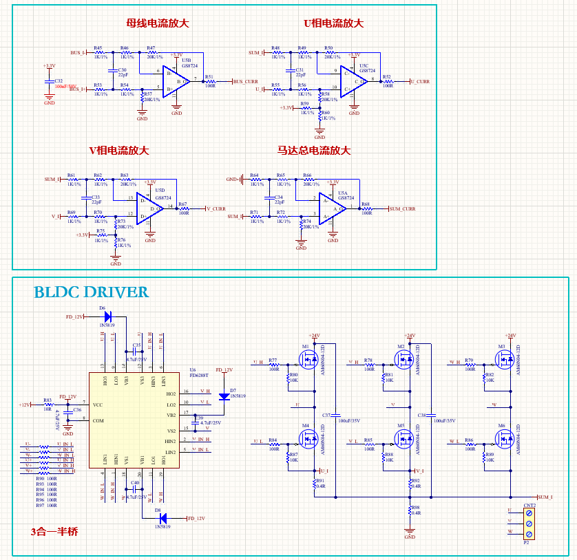
N-channel driver requires a separate pre-driver chip
-
Operational amplifier for current acquisition and amplification
-
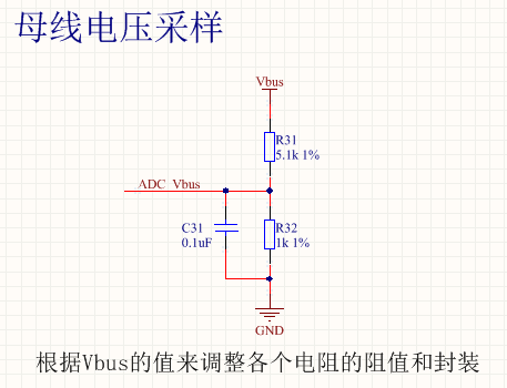
Bus voltage acquisition
-
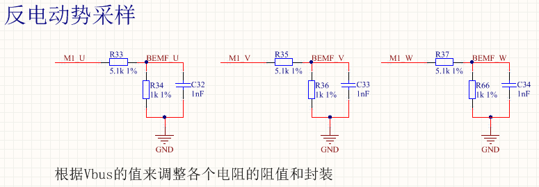
MCU and back EMF sampling circuit
-
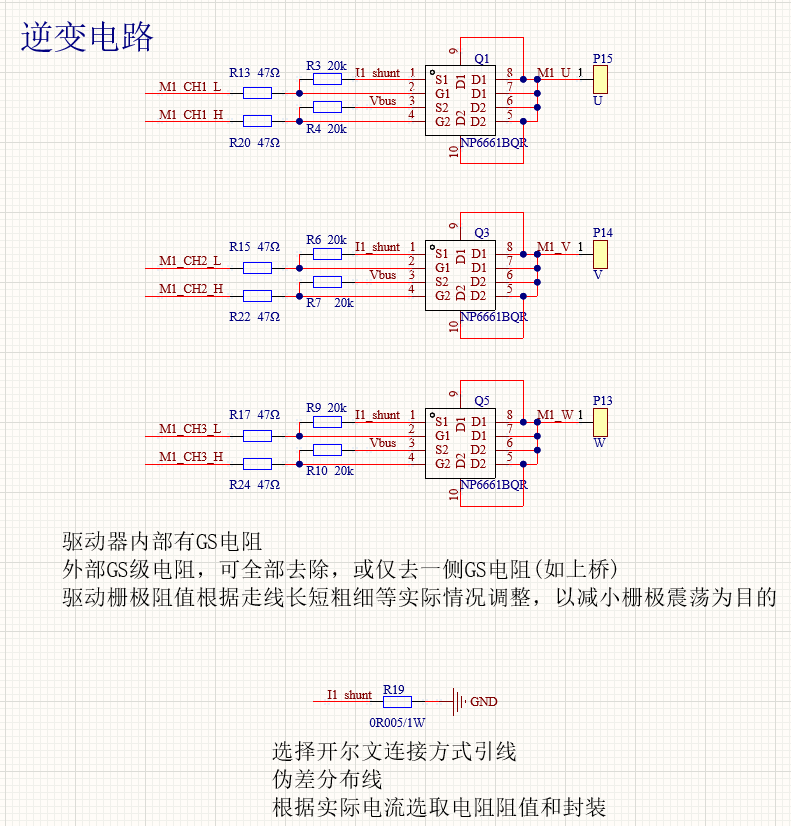
Inverter circuit
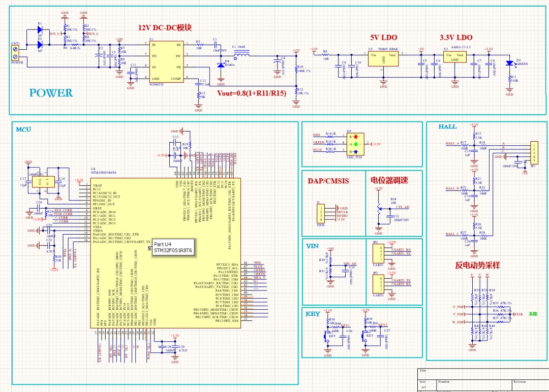
The above is the <span>most basic</span> brushless motor drive circuit. With this circuit, all functions can definitely be achieved, but each functional module is an independent circuit. The overall solution will first be costly <span>and not cheap</span>, and second, it will be relatively large.
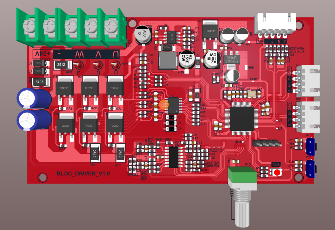 The size of the above board is 120*69mm, of course, it can be smaller, but it won’t be super small.
Is there a more <span>concise</span> solution? For example, integrating many of these modules into a single chip.
Of course, market demand will promote faster R&D upgrades. With the increasing demand for miniaturized brushless drives in many products, such as smart toothbrushes, micro fans, hair dryers, etc., corresponding micro and cost-effective solutions have emerged.
Now let’s think about which of the above seven circuit parts can be combined?
- MCU is definitely needed,
<span><span>LDO integrated into the MCU</span></span>is also feasible, as the current required by the MCU is very small, and 24V power supply can still be achieved - The pre-driver part, which is originally a chip, must be arranged
<span><span>to be packaged with the MCU</span></span> - Operational amplifier, this is also fine, as some MCUs already integrate operational amplifiers and comparators
- Bus voltage ADC acquisition, this goes without saying
- Back EMF sampling, just a few resistors and capacitors, the circuit is placed outside
- MOS inverter circuit, this cannot be integrated, nor is it necessary
Looking at it this way, a complete PCBA can consist of MCU + inverter circuit + back EMF sampling, while the other circuits (high-voltage LDO + pre-driver + operational amplifier) are all integrated within the chip. Is there such a chip solution?
Do you remember the smallest series of domestic chips we mentioned a few days ago?
The smallest motor MCU with built-in pre-driver op-amp, the smallest USB3.0 HUB, and a review of various domestic smallest chips in niche fields (click to read)
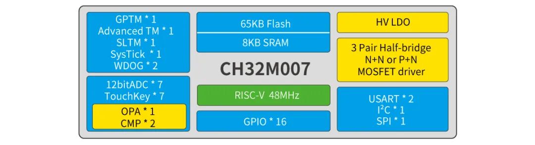
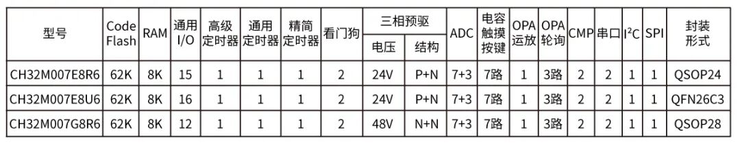
At that time, we applied for the smallest size CH32M007E8U6, 3*3mm. Now that we have played with it for a while, I would like to share some insights.
Click to follow and star Eefocus
Scan the code and reply with “chip, MCU” keywords to join the industry group and receive reports
CH32M007 is an industrial-grade motor microcontroller designed based on the Qingke RISC-V core, supporting a system main frequency of 48MHz and single-wire debugging.
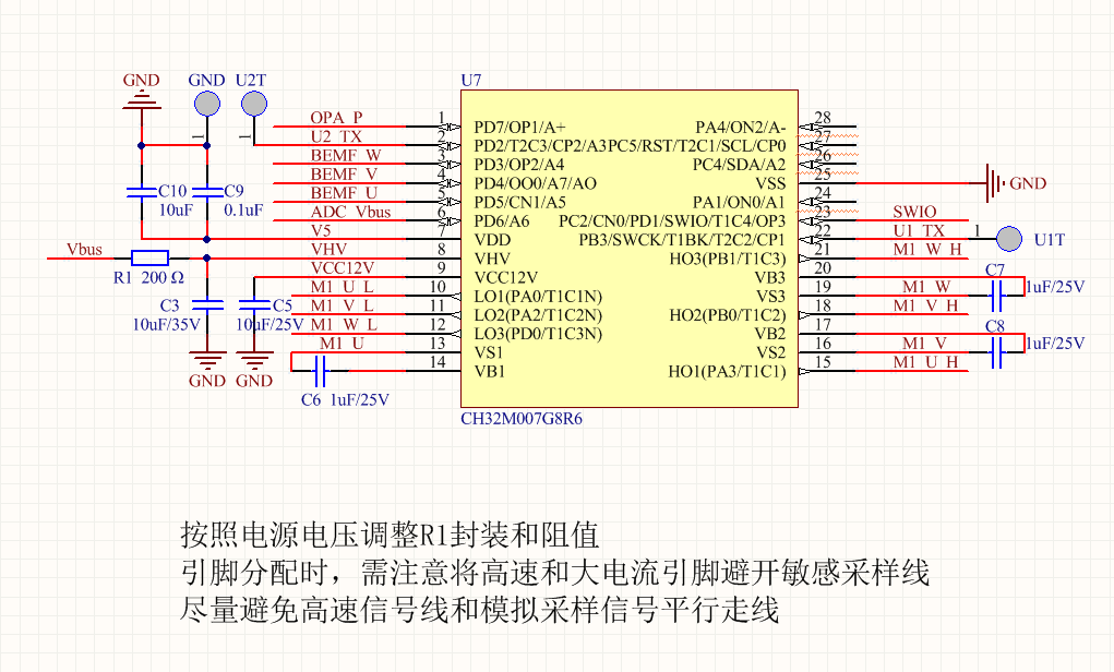
It has a built-in 12-bit ADC with a sampling rate of up to 3Msps.
It includes a <span>high-voltage slew rate operational amplifier OPA</span>, supporting 3-channel polling and single or dual resistor current sampling schemes.
It can be used for sensor-based positioning, ADC sampling, or comparator sensorless positioning, with single or dual resistor sampling motor schemes.
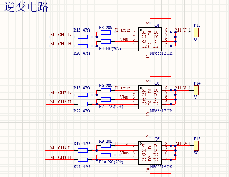
CH32M007G8R6 has a built-in <span>48V three-phase dual N pre-driver</span> and bootstrap diode along with a high-voltage LDO, allowing the inverter circuit to be directly connected to the MCU.
This chip is indeed quite versatile, with all the conventional features needed, specifically designed for motor control.
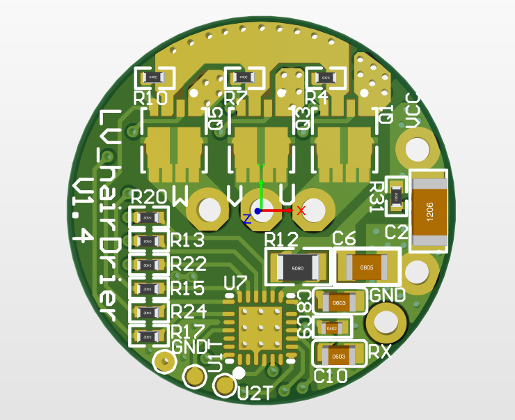
Let’s take a look at the PCB demo, this is a brutal hair dryer solution, with a size of 31.5 * 25.5mm, very small. The entire board, apart from the chip and MOSFETs, only has resistors and capacitors, and can easily reach 100,000 RPM.
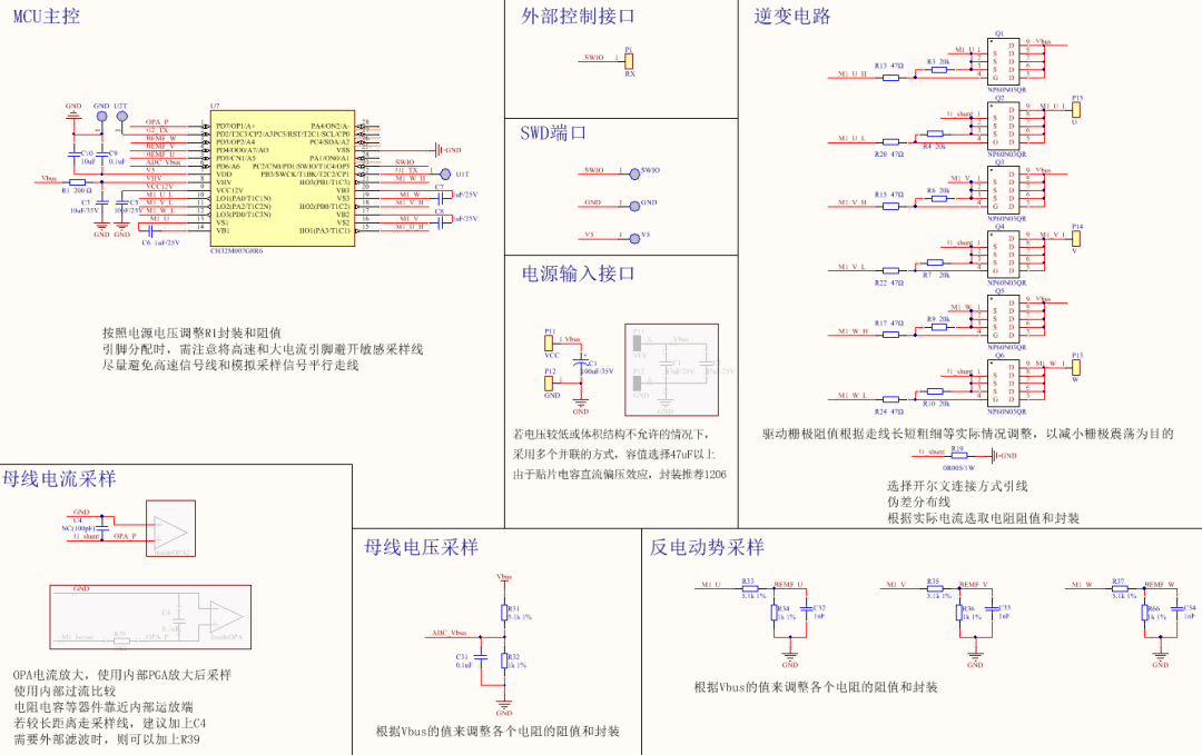
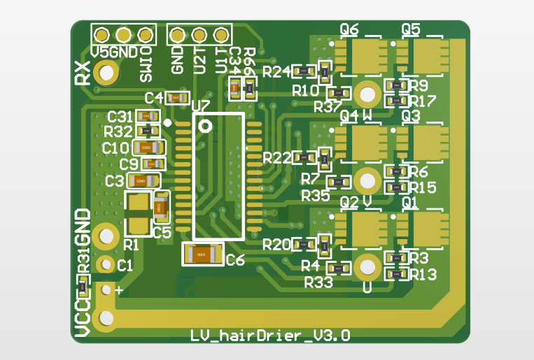
The above solution uses a three-phase dual N-type pre-driver, so the MCU needs a high-side bootstrap circuit.
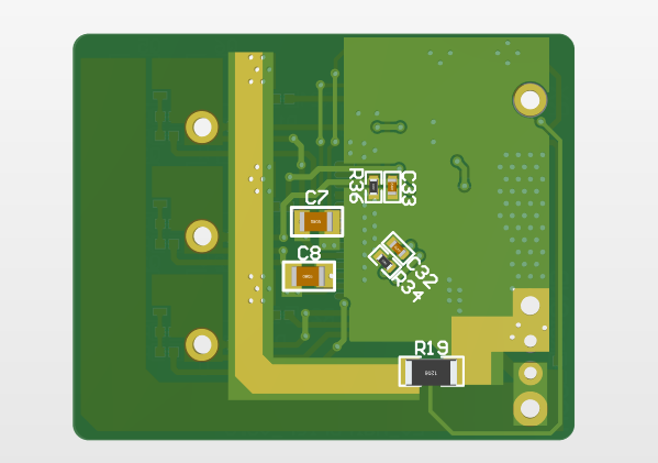
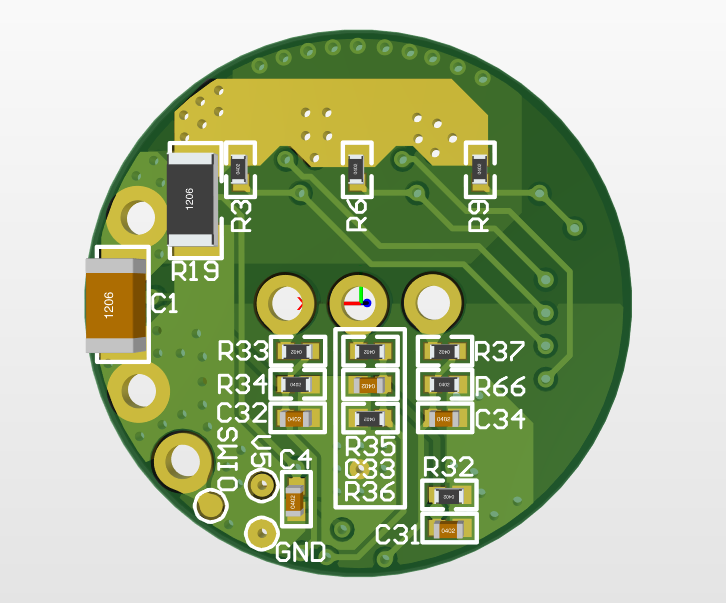
There is also a PCB area-saving, cost-saving solution, <span>three-phase P+N type pre-driver. The CH32M007E8U6 I have on hand has a PCB diameter of less than 2cm, which is more than enough for strict size requirements.</span>
This means using a P-channel MOSFET for the upper switch. The P-MOS upper switch conducts when Vgs is negative, eliminating the need for an additional bootstrap circuit, making the high-side drive logic simpler, thus reducing the chip cost further.
However, while the upper switch using a P-channel MOSFET simplifies the circuit, PMOS has a lower carrier mobility than NMOS electrons, which limits the <span>switching speed</span> response compared to NMOS under the same driving voltage.
The second issue is the on-resistance; under the same conduction capability, PMOS usually requires a larger W/L (width/length) ratio, resulting in <span>higher on-resistance.</span>
Thus, these two points <span>limit the PMOS solution</span>, but the overall cost is lower, making it sufficient for applications like toys and small fans. Let’s take a look at the <span>PMOS inverter circuit.</span>
The PCBA size can also be made smaller, with a circular board used in hair dryers, having a <span>diameter of only 19mm, which is particularly small.</span>
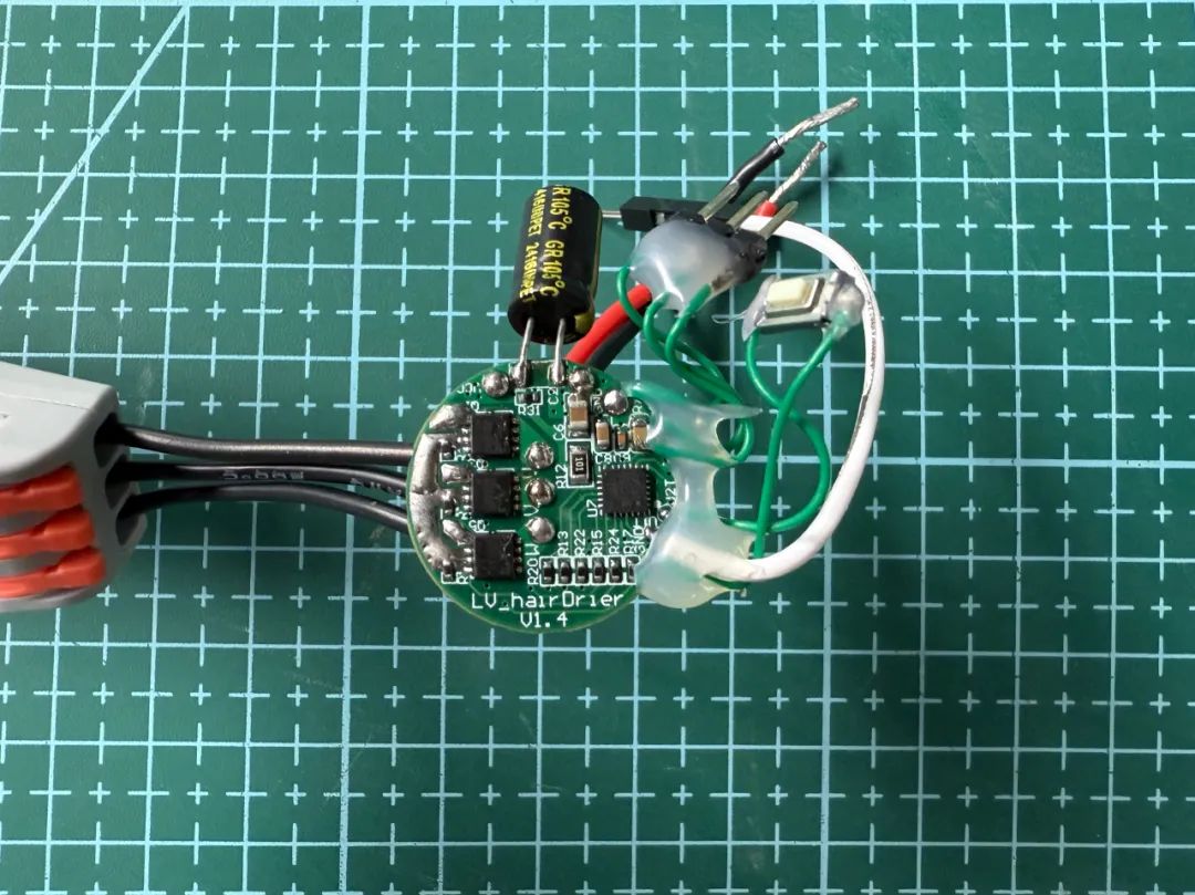
Let’s take a look at the physical product
PCB engineering files:
Files shared via cloud drive: LV_hairDrier_V3.0.zip
Link: https://pan.baidu.com/s/1enAQIjZYllYDGxTmFpFmHQ?pwd=tyd9 Extraction code: tyd9
END
Note: The cover image of this article comes from Freepik, self-made by the author, and publicly authorized media materials.
Welcome to leave comments and exchange in the comment area!


Industry Community