1.Xilinx FPGA Development Overview
1.Xilinx FPGA Development Timeline
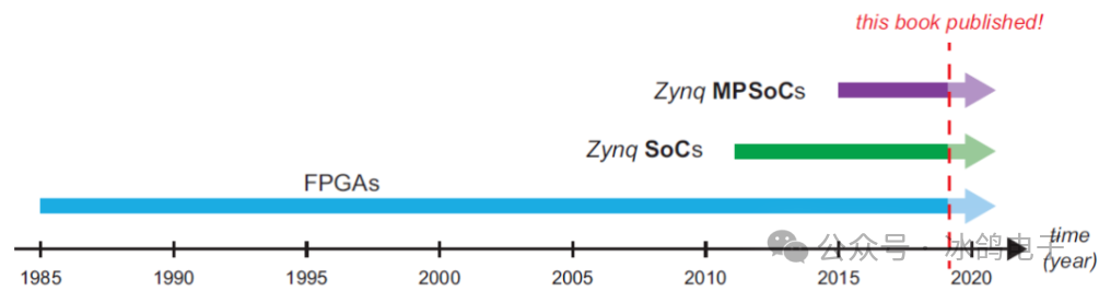
Xilinx(Xilinx) FPGA was officially acquired by AMD on February 15, 2022, through a full stock transaction. The following article will continue to refer to Xilinx FPGA.
2.Xilinx FPGA Classification
Xilinx FPGA products are classified by process node into 16nm, 20nm, 28nm, and 45nm; by industry, they are classified into industrial, consumer, automotive, defense, and aerospace grades.
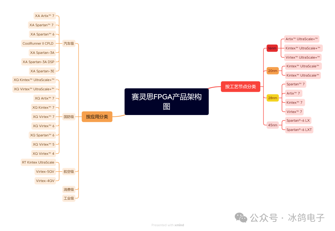
Xilinx #FPGA is mainly divided into four series based on different processes and logic resources: Series 6, Series 7, UltraScale, and UltraScale+.
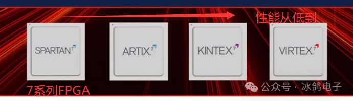
Series 7 is a generation of FPGA products launched by Xilinx in 2011, including Artix-7, Kintex-7, Virtex-7, and Zynq-7000 (which integrates ARM hard cores and FPGA with equivalent performance to Series 7). There are four sub-series.
Series 7 uses a 28nm process and features high performance, low power consumption, and high integration. Series 7 supports various protocols and interfaces, such as PCIe Gen2/3, Ethernet, USB, SATA, etc. It also provides a rich set of IP cores and development tools, making it easy for users to design and verify their applications.
The UltraScale series is a generation of FPGA products launched by Xilinx in 2014, including Kintex UltraScale, Virtex UltraScale, Kintex UltraScale+, and Virtex UltraScale+. The UltraScale and UltraScale+ series are essentially upgrades and enhancements of the resource quantity and bandwidth based on the Xilinx 7 series, improving the process and reducing power consumption.
The UltraScale series uses a 20nm or 16nm process, featuring higher performance, lower power consumption, larger capacity, and more functions. The UltraScale series supports more protocols and interfaces, such as PCIe Gen3/4, 100G Ethernet, Interlaken, etc. It also provides more advanced IP cores and development tools, supporting advanced design methods and technologies such as SDx, SDAccel, and SDSoC.
In addition, there are RFSOC FPGAs that integrate ADC/DAC and SoC, and automotive-grade FPGA series XA, etc. Due to limited personal exposure, I will not elaborate further; please search for more information if interested.
3.Resource Overview
Xilinx’s FPGA architecture started with only 64 flip-flops and 3-input lookup tables (LUTs) to implement logic functions. In terms of FPGA scale, logic density is measured in “logic cells”..
The basic FPGA structure of Xilinx is still a two-dimensional array of digital logic elements grouped into CLBs. Each CLB contains a small number of flip-flops and LUTs, where LUTs are used to implement Boolean logic functions, small block memory, and shift registers. From a lower level perspective, the composition of CLBs has evolved over time, with modern CLBs containing more logic resources than earlier CLBs.
2. Taking 7 Series FPGA (kintex-7) as an example
1.7 Series FPGA Classification
Xilinx has a wide variety of FPGA products, among which the 7 Series FPGA products were released in 2010. This series of FPGAs uses a more advanced 28nm process, with internal logic resources significantly improved compared to previous FPGAs, and device power consumption has been greatly reduced compared to earlier FPGAs.
Xilinx’s 7 Series FPGAs are divided into four sub-series based on different customer application needs: Spartan7 series, Artix7 series, Kintex7 series, and Virtex7 series.
1) Spartan series: Positioned in the low-end market, the latest device is Spartan7, which uses a 28nm process, while previous Spartan6 was 45nm. This series of devices is affordable, with relatively small logic scale.
2) Artix series: Xilinx launched the Artix series FPGA products as a transitional product between the low-end Spartan and mid-to-high-end Kintex series FPGAs, especially in terms of communication interfaces, the Artix series has significant advantages over Spartan. Therefore, if the design requires not only logic resources but also advanced high-speed interfaces, consider the Artix series.
3) Kintex and Virtex series are Xilinx’s mid-to-high-end products, including the 28nm Kintex7 and Virtex7 series, the 20nm Kintex7 UltraScale and Virtex7 UltraScale series, and the 16nm Kintex7 UltraScale+ and Virtex7 UltraScale+ series. They have rich high-speed interfaces, mainly used in high-end fields such as communications, radar, signal processing, and IC verification.
4) Fully programmable SoC and MPSoC series, including Zynq-7000 and Zynq UltraScale+ MPSoC series FPGAs, which embed ARM Cortex series CPU cores.
Application Development Tools: Vivado (new) and ISE (old)
2.Kintex-7 Naming Convention
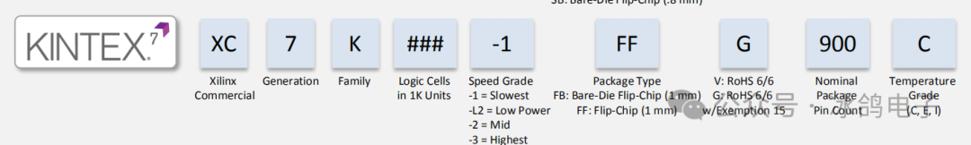
XC —- Xilinx Company (xilinx commercial)
7 —- Generation
K —- Family (Family) For example: kintex
### —- Logic (LUT) Capacity (logic cells in 1k units)
-1 —- Speed Grade (Speedgrade -1 slowest –l2 low power -2 mid)
FF —- Package Type (packageType FF Flip-chip)
900 —- Pin Count (nominalpackage pin count)
C —- Temperature Grade (temperature grade)
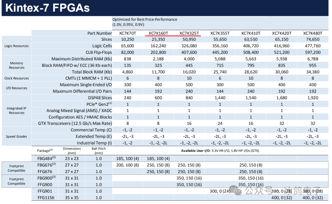
3.Kintex-7 Resources
Traditional FPGAs mainly consist of IOB, CLB, BRAM, and rich internal wiring; the internal structure of Kintex-7 FPGAs compared to traditional FPGAs embeds units such as DSP48E1, PCIe, GTX, XADC, and high-speed I/O ports, greatly enhancing the performance of the FPGA.
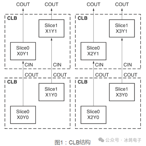
4.CLB Overview
CLB (Configurable Logic Block) is the basic logic unit of Xilinx FPGAs, each CLB contains two slices, each slice consists of 4 six-input LUTs, 8 D flip-flops, and multiple MUXes (multiplexers). The two slices in the same CLB do not have direct line connections and belong to two different columns. Each column has independent fast carry chain resources.
5.MGT Overview
MGT (Multi-gigabit transceiver): A bidirectional serial transmitter, MGT is an abbreviation for high-speed serial transceiver modules. Xilinx integrates different numbers of MGTs in its Artix7, Kintex7, and Virtex7 to achieve high-speed serial communication between the FPGA and the outside world, and assigns new names based on the supported line speeds. Additionally, Spartan7 does not have MGT. In Artix7, MGT is called GTP; in Kintex7, MGT is called GTX; in Virtex7, MGT is called GTX/GTH/GTZ;
The performance of the three types of high-speed serial transceivers in the 7 series is as follows:
GTH: 500Mb/s~13.1Gb/s
GTX: 500Mb/s~12.5Gb/s
GTP: 500Mb/s~6.6Gb/s
GTZ: Maximum line speed 28.05Gb/s
Regardless of whether it is GTP, GTX, or GTH, they are composed of three modules:
1)Clock Module
2)Data Transmission Module
3)Data Reception Module
GTX transceivers support these usage modes: PCI Express, versions 1.1/2.0/3.0, 10GBASE-R, Common Packet Radio Interface (CPRI™), SATA, SFP+;
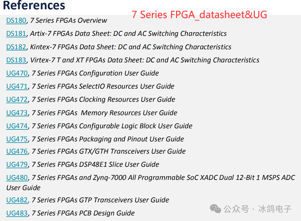
6.7 Series FPGA Learning Resources
Xilinx’s official documentation can be searched and downloaded through the installation of the Xilinx Documentation Navigator, abbreviated as docnav. This software is automatically installed when installing Vivado, and can also be installed separately through the installation package.
Xilinx’s documents can be mainly divided into the following categories, distinguished by their abbreviations.
|
Starting Letter |
Meaning |
Description |
|
ds |
data sheet |
Electrical characteristics of the device |
|
ug |
user guide |
Introduction to chip resources |
|
wp |
white paper |
Authoritative basic knowledge |
|
bg |
Package Specifications |
Packaging information |
|
xapp |
application note |
Guidance for specific implementations |
Below are some official PDF documents for learning about the Kintex-7 series FPGAs.