Common PCB Issues
Quality Issues and Solutions
(Part 1)
In disputes between electronic product manufacturers and PCB suppliers, quality issues with PCBs have become a high-risk factor that triggers supply chain disputes. Since 2018, the PCB legal team at Maoda Law Firm has handled thousands of various contract disputes arising from quality issues. These real legal disputes not only concern the economic interests of enterprises but also expose many common quality problems in the PCB industry. This article analyzes common quality issues in PCB products based on the legal practice experience of the law firm, aiming to provide risk prevention guidance and rights protection advice for enterprises and practitioners.
01
CAF
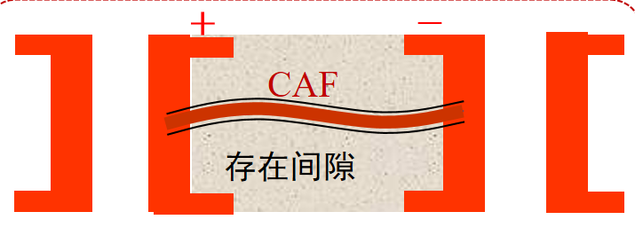
CAF (Conductive Anodic Filament) refers to the phenomenon of “copper ion migration”.
It refers to the migration of metal ions along the interior or surface of insulating materials under humid, high-temperature, and electric field conditions, forming conductive pathways.
1
Necessary Factors for CAF Formation:
① Presence of conductive and mobile metal particles such as copper;
② Humid environment that serves as a carrier for ion migration;
③ Presence of channels for ion migration;
④ Presence of an electric field or voltage difference;
2
The Four Major Causes of CAF
① Material issues: High moisture absorption of the substrate (e.g., standard FR-4);
② Design flaws: Too narrow spacing between traces;
③ Process failures: Rough drilling, insufficient lamination, gaps become highways for ions!
④ Environmental factors: High temperature and humidity;
3
Three Ways to Eliminate CAF!
① Material upgrade: High Tg materials, CAF-resistant resins to block ions at the source!
② Design optimization: Ensure conductor spacing (e.g., >0.3mm)! Arrange solder mask/CAF-resistant coatings properly!
③ Process control: Laser drilling, vacuum lamination, etc.;
④ Environmental management: Stay away from high temperature and humidity environments;
02
PCB Delamination and Bubbling
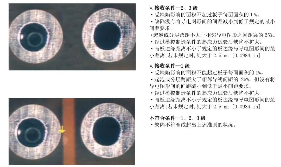
PCB delamination and bubbling refer to the failure of the bonding strength between various layers of the PCB (such as copper foil, resin substrate, prepreg, etc.), leading to interlayer separation and the formation of local bubbles or bulges.
1
Specific Manifestations:
· Abnormal appearance: Local bulging on the board surface.
· Internal defects: Bubbles or voids visible between layers through X-ray or ultrasonic inspection.
· Location characteristics: Commonly found around vias, in areas with dense copper foil, at board edges, or in areas with concentrated thermal stress.
2
Cause Analysis:
The fundamental cause of delamination and bubbling is insufficient bonding strength between layers, with specificinducing factors including:
① Material issues: Poor substrate quality, adhesive failure, improper copper foil treatment, etc.
② Process defects: Insufficient lamination temperature or pressure, inadequate post-drilling treatment, etc.
③ Design factors: Uneven copper foil distribution, defects in blind/buried hole design, etc.
④ Environmental impacts: Excessively high humidity in the production environment or prolonged exposure to humid and hot conditions, leading to moisture absorption and thermal expansion of the substrate causing delamination.
3
Impacts and Consequences:
“Mild cases lead to signal interference, severe cases can cause direct short circuits! A bulging board can render the entire machine scrap in no time!”
Delamination and bubbling have significant negative impacts on PCB performance and end products:
Poor appearance, decreased electrical performance, reduced mechanical strength, and reliability risks.
4
Prevention and Improvement Measures:
① Material optimization: Use low moisture absorption, high heat resistance substrates.
② Process control: Adjust temperature, pressure, and time according to material characteristics; strengthen post-drilling treatment; pre-bake and dehumidify before lamination.
③ Design improvements: Optimize copper foil distribution; adopt stepped blind hole designs to reduce resin filling difficulties.
④ Environmental management: Control humidity in the production environment to prevent substrate moisture absorption.
⑤ Strengthen inspection: Introduce thermal stress testing and ultrasonic scanning (SAT) for comprehensive inspection.
03
Halo Effect
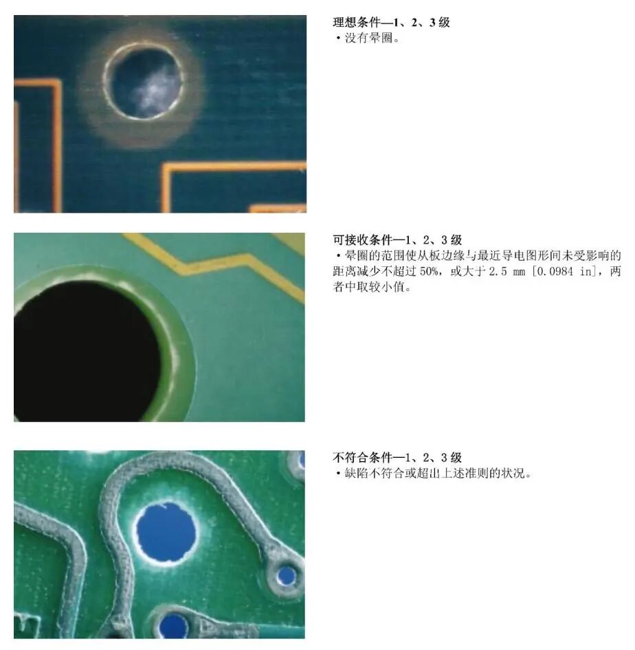
The halo effect refers to the damage or delamination phenomenon on the internal or surface of the substrate caused by mechanical processing on the PCB, typically manifested as white or light-colored ring-like marks around drilled holes, cutting edges, or other processing areas, presenting a whitening phenomenon resembling a “halo”.
The formation of halos is usually related to multiple factors including materials, processes, and environments.
1
Potential Hazards of Halo Effects on PCB Performance and Reliability:
1. Decreased electrical performance, leading to leakage or short circuits.
2. Reduced mechanical strength, with delaminated areas prone to further cracking, causing solder joint detachment or circuit breakage.
3. Long-term reliability risks.
4. Appearance and customer trust issues, as obvious appearance defects may lead to customer rejection.
2
The core of halo acceptability lies in risk control:
According to IPC industry standards, acceptable conditions are: the range of halos does not reduce the distance from the board edge to the nearest conductive pattern by more than 50%, or is greater than 2.5 mm.
That is, only appearance defects, no functional impact, no risk of delamination expansion, and no impact on electrical performance, complying with customer or industry standards.
04
No Copper in Holes
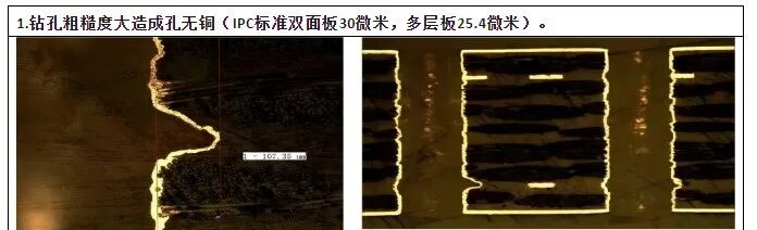
No copper in holes refers to the situation in PCB production where the hole walls are not fully plated with copper, leading to poor conductivity. This is specifically manifested as discontinuous or completely absent copper layers within the holes, usually occurring in through-holes and blind holes.
1
Main Causes of the Problem:
① Process stages: Such as drilling quality issues, improper control of the chemical copper deposition process, inadequate cleaning, defects in the electroplating process, etc.;
② Substrate and environmental factors: Such as the quality of the substrate material;
③ Design defects: Such as unreasonable hole diameter design.
2
Impacts:
Electrical performance failure;
Reduced assembly yield, leading to cold solder joints or detachment;
Increased costs and scrap rates;
3
Prevention and Solutions:
The occurrence of no copper in holes is multifaceted, with root causes concentrated in critical process stages such as drilling, copper deposition, and electroplating. Systematic control is required across the entire process, including design, materials, processes, and inspections. This includes using high-quality raw materials, optimizing drilling and cleaning processes, accurately controlling electroplating parameters, regularly maintaining equipment, and implementing strict quality inspection standards.
05
Thin Copper in Holes
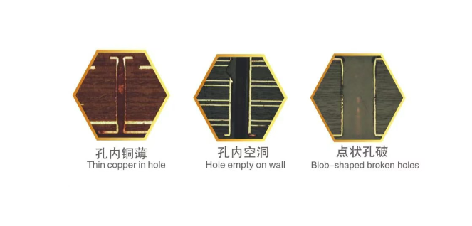
Thin copper in holes refers to the situation where the copper layer thickness on the hole walls does not meet design or industry standards. The thickness of copper in holes is one of the important factors affecting the reliability and lifespan of printed circuit boards, and is primarily manufactured according to IPC standards and customer requirements.
1
Causes:
The causes of this quality issue are similar to those of the no copper problem, arising from process stages, substrate, environmental factors, and design defects.
However, it is more insidious than the no copper phenomenon, as the defective holes often appear conductive during electrical testing, requiring the use of low-resistance testing machines to effectively detect.
2
Thin copper in holes has a progressively deteriorating impact on PCB performance:
① Abnormal electrical performance: Increased conduction resistance, insufficient current carrying capacity, high-frequency signal distortion;
② Insufficient mechanical strength: Tear of through-hole, wall breakage;
③ Solder reliability issues: Poor solder wetting, leading to cold solder joints or voids due to uneven heat conduction;
④ Long-term reliability failures: Copper cracks expanding after thermal cycling tests, delamination of copper layers from substrates after damp heat aging;
06
Legal Services Offered
As one of the core legal products of the PCB industry lawyer team at Maoda Law Firm, this product provides PCB enterprises with
various litigation and non-litigation solutions for quality disputes:
(1) Review contracts and improve provisions related to quality standards, compensation, and handling plans;
(2) Provide risk assessment and reports for quality disputes;
(3) Develop response mechanisms for product quality disputes for enterprises;
(4) Formulate rights protection plans for product quality disputes for enterprises;
(5) Represent identification procedures arising from quality disputes;
(6) Represent negotiations, discussions, and settlements of quality disputes;
(7) Represent administrative investigations, administrative litigation arising from quality disputes;
(8) Represent arbitration and litigation arising from quality disputes;
(9) Other legal matters related to quality disputes;
07
PCB Lawyer Team

Wang Yiliang Lawyer
Head of the PCB Industry Lawyer Team
24 years of practice experience
Since starting practice, he has primarily served PCB enterprises, focusing on legal services for PCB enterprises in the past five years, handling numerous legal matters in the PCB industry, including quality disputes that exceeded client expectations, establishing long-term cooperative relationships with over 50 PCB enterprises.

Zheng Fei Lawyer
Senior Lawyer in the PCB Industry
Central South University of Economics and Law
Dual degrees in Law and Accounting
Graduated from Central South University of Economics and Law, majoring in law and minoring in accounting, obtaining dual bachelor’s degrees in law and accounting. Proficient in legal business and equipped with solid economic knowledge such as accounting. Since starting practice in 2018, he has specialized in commercial arbitration and litigation for enterprises, with unique case handling experience in arbitration and litigation matters, especially in PCB industry quality disputes, successfully representing numerous civil and commercial cases including contract disputes (including PCB quality disputes), sales contract disputes, private lending disputes, and lease contract disputes.
08
Successful Cases
Maoda PCB Case丨A must-read for enterprises! How to win a lawsuit with an unpaid invoice without a stamped reconciliation statement? Email evidence + key contract clauses should be written this way.
Maoda PCB Case丨Litigation Guide – How to Address Quality Issues in Contract Disputes?Maoda PCB Case丨Counterclaiming the defendant, how Maoda lawyers analyze equipment quality issues in sales contract disputes.
Maoda PCB Case丨How to claim losses caused by quality issues?
Maoda PCB Case丨In this contract dispute case, both parties were plaintiffs and defendants due to PCB quality issues. How did Maoda lawyers help the client win in this complex case?
Maoda PCB Case丨Because of PCB quality issues, the plaintiff became the defendant? How did Maoda lawyers turn the tide, and how did the court rule?
Maoda PCB Case丨From processing contract disputes, the importance of evidence retention regarding PCB quality issues.
Maoda PCB Case丨How to refute quality issues in PCB contract disputes? Maoda lawyers offer advice.
Maoda PCB Case丨An electronic company in Shenzhen claimed deductions due to poor PCB materials. How did Maoda lawyers reveal the winning strategy to recover payments?
Welcome to Contact
Maoda Lawyers
Ma
oda
Law
yers
This article may not be used for other purposes without the written consent of this law firm.
Unauthorized reproduction or use is prohibited.
If you have any questions about the content of this article, please feel free to contact us.