


SMT Top Networking Circle
A professional circle for sharing networking resources and achieving career advancement.

New Platform 2020


1. Purpose The total cost of a product is determined by 60% from the initial design; 75% of manufacturing costs depend on design specifications and guidelines; and 70-80% of production defects are caused by design issues. Therefore, to standardize the manufacturability review of new products at various stages of the initial design, ensuring that the review is evidence-based, and to ensure that new products meet requirements for efficiency, cost, quality, etc., this specification document is established to shorten the R&D cycle of new products and enhance product quality and competitiveness.2. Scope Applicable to manufacturability design reviews of all new SMT products at various development stages.3. References IPC-A-610F, Acceptability of Electronic Assemblies; IPC2221, Generic Standard on Printed Board Design; IPC-7351—Surface Mount Design and Pad Layout Standard General Requirements.4. Terminology
1. SMT (Surface Mount Technology) refers to an electronic assembly technology that uses automatic placement equipment to mount surface-mounted components to specified positions on the PCB surface.
2. THT: Through Hole Technology (THT) refers to through-hole insertion technology.
3. PCB (Printed Circuit Board) refers to a circuit arranged with copper on a printed circuit substrate.
4. PCBA (Printed Circuit Board Assembly) refers to a circuit board assembly completed using surface mount technology.
5. SMD (Surface Mount Device) refers to surface-mounted components, which differ from previous through-hole components and are mounted on the surface of the PCB.
6. SOP (Small Outline Package) is a surface-mounted IC with approximately 8-40 pins on both sides of a rectangular body, with lead pitches of 0.5mm, 0.65mm, 0.8mm, 1.27mm, etc.
7. QFP (Quad Flat Package) is a surface-mounted IC with approximately 100-250 pins around a square or rectangular body, with lead pitches of 0.4mm, 0.5mm, 0.65mm, 0.8mm, etc.
8. BGA (Ball Grid Array) is a package with ball-type electrodes, with lead pitches of 0.8mm, 1.27mm, etc.
9. Wave Soldering is a process where molten soft solder is pumped to form a solder wave, allowing a printed board with pre-installed electronic components to pass through the solder wave for soldering.
10. Reflow Soldering differs from previous wave soldering, as it involves applying solder paste to the PCB and then heating it for soldering.
11. Fiducial Mark: Used in SMT equipment such as screen printers and chip mounters to identify and correct the coordinates of the substrate or components.
12. ICT: In-Circuit Test, which checks for shorts/opens and various component characteristics after soldering.
13. T/P: Test Point, designed for alternative leads to facilitate contact during ICT or Function Test JIG usage.
5. Responsibilities 5.1 R&D Engineers: Responsible for initiating manufacturability review requests during the design phase, providing relevant technical documents such as PCB files, assembly drawings, debugging plans, BOM, etc., to the NPI engineers for review, and responsible for formulating and executing improvement plans for design issues identified during the review. 5.2 NPI Engineers: Upon receiving the above materials from R&D during the new product development phase, they begin organizing reviews with procurement engineers and R&D engineers, producing review reports. 5.3 Process Engineers: Responsible for executing manufacturability and testability technical reviews of the product, identifying issues and suggesting improvements. 5.4 Procurement Engineers: Responsible for executing the review of the product’s material procurement feasibility, identifying issues and suggesting improvements.
I. PCBA Processing Procedure Design
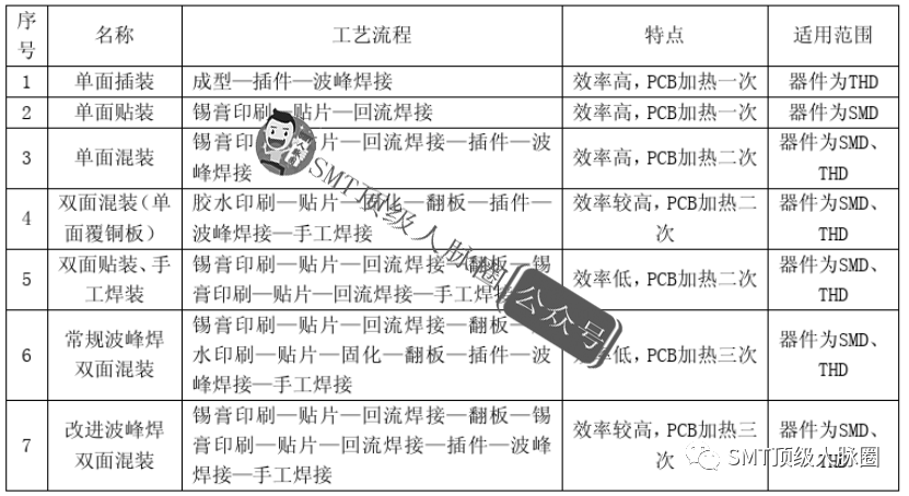
The layout of components on the manufactured board should ensure a reasonable processing sequence to improve processing efficiency and yield. The processing flow for PCB layout should maximize processing efficiency. The preferred sequence of processing technology is: single-sided component mounting on the component side—component side mounting, mixed insertion (top-side insertion and wave soldering simultaneously)—double-sided mounting—component side mounting, mixed insertion, and soldering on the component side. The seven mainstream processing flows for common PCBA are as follows:
II. PCBA Design Section
1. Positioning Hole Design:
1.1 Installation holes should be selected based on actual needs (at least one pair of positioning holes should be set on the long side). Generally, a diameter of Φ4.5mm is chosen, with a flat washer position set on the silkscreen layer outside the hole, corresponding to an M3 combination screw with an outer diameter of Φ7mm. Grounding installation holes should be set as metallized holes, with the installation hole size for M4 combination screws being Φ4.5mm and the flat washer size being Φ8mm. 1.2 The distance from the hole center to the PCB edge should not be less than 5mm, and the distance from the edge of the flat washer to the edge of the component should not be less than 1mm. No traces, component pads, or vias should be laid out within this range. 1.3 Generally, the hole diameter for installation holes should be 0.5mm larger than the diameter of the installation screws.2. Process Edge Design:
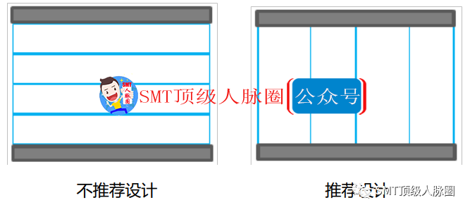
2.1 For PCBs with irregular shapes or components within 4mm of the PCB edge, process edges need to be added to ensure sufficient gripping edges for the PCB. 2.2 The process edge should connect to the PCB using postage holes or V-shaped grooves. 2.3 The copper foil within the process edge should be designed in a grid pattern to increase transmission friction. 2.4 No machine-mounted components should be arranged within the process edge, and the physical presence of machine-mounted components should not extend into the process edge or above it. 2.5 The width of the process edge should be at least 3mm, with at least two symmetrical edges. To prevent the PCB from getting stuck during machine transport, the corners of the process edge should be rounded.3. PCB Panel Design: 3.1 When the size of a PCB unit is < 80mm×80mm, panelization is required. 3.2 The size of the panel should facilitate manufacturing, assembly, and testing processes without causing significant deformation. 3.3 Interconnections between PCB segments in the panel should use double-sided V-CUT or postage hole or slot designs. 3.4 PCB segments should be arranged in the same direction during panel design, with each small board arranged on the same side. 3.5 Generally, the number of V-CUT lines parallel to the PCB transport edge should be ≤3 (exceptions can be made for elongated boards). As shown below:
3.6 The number of panels should not exceed the range of the placement machine, ideally within 250mm×250mm, to facilitate quality and efficiency control during production.
4. Reference Point Design:
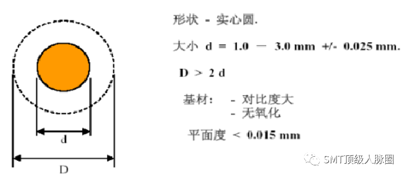
4.1 Reference MARKs for the panel should be added to the diagonals of each small board, generally two to three, with the same shape; for boards that are too small or have densely packed components that cannot have MARK points laid out according to specifications, they can be arranged on the edges of the entire panel after panelization. 4.2 The size requirement for MARK points: d = 1.0mm, which can also be square; all MARKs on the PCB should be consistent, and the area around the MARK point should be free of solder mask layers, with a range greater than 2mm.
4.3 The position of the MARK point should be at least 3.5mm from the PCB edge to avoid being caught by the machine’s track, and there should be no other similar shapes within a 3mm range; the background within 3mm should be consistent. 4.4 For ICs with pin centers less than 0.65mm, reference points should also be set to ensure accurate alignment during component placement.
5. Silkscreen Design:
5.1 The PCB should have complete information about the manufacturer, PCB number, version number, production cycle, high voltage hazard, and some special purpose markings, clearly and prominently positioned. 5.2 All components, test points, installation holes, and heat sinks should have corresponding silkscreen markings and position numbers. 5.3 Silkscreen characters should follow the principle of left to right, top to bottom; for polarized components, the direction should be kept consistent within each functional unit for ease of operation and inspection. 5.4 The markings on the PCB must be completely consistent with the identifiers in the BOM list. 5.5 Silkscreen should not be on pads, and silkscreen should not overlap, intersect, or be obscured by components, avoiding defects caused by vias. 5.6 The thickness, direction, spacing, and accuracy of silkscreen should be standardized; all sizes of markings and characters on the board should be uniform, and if marking positions are limited, they can be marked in other empty areas with arrows indicating direction. 5.7 The PCB should reserve a position for “labels” and draw a silkscreen box; there should be no other silkscreen markings or test points below the “label.” 5.8 Through-hole ICs and connector components should be marked with pin functions or numerical sequences on both the TOP and BOTTOM sides; for components with many pins, numerical sequences or functions can be marked intermittently, but at least the first and last pin numbers should be provided.