Source: Semiconductor All Explained
Original Author: Yuan Yuan De Yuan
This article introduces some basic concepts in the semiconductor field in a lively and easy-to-understand manner.
Semiconductors are a key industry developed by the country in recent years. What exactly is a semiconductor?
All objects in life can be roughly divided into three categories based on conductivity: conductors, semiconductors, and insulators. This is easy to understand; an object either conducts electricity, does not conduct electricity, or conducts electricity to some extent. It is precisely this ambiguous and unclear material that gives physicists different room for exploration.
Materials with absolute conductivity or non-conductivity are not interesting; what is interesting is the change in conductivity under different conditions.
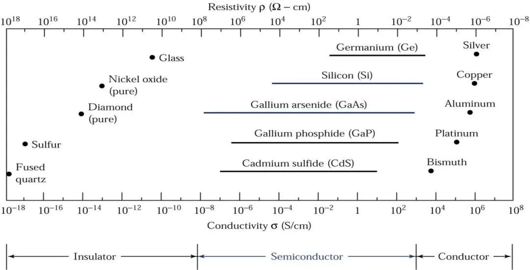
Let’s look at a diagram to visualize the conductivity of materials:
Based on conductivity, materials can be divided into:
Insulators: Very low conductivity, approximately between 20E−18S/cm and 10E−8S/cm, such as fused quartz and glass;
Conductors: Higher conductivity, between 10E4S/cm and 10E6S/cm, such as aluminum, silver, and other metals.
Semiconductors: Conductivity lies between insulators and conductors.
Common elemental semiconductors in nature include silicon and germanium. It is said that germanium-based semiconductors were discovered and used even before silicon-based semiconductors, but the natural advantage of silicon is its low cost!
Common sand in nature contains a large amount of silicon!
Even though there is a lot of silicon sand in nature, the impurities contained in silicon sand are too many, and the defects are too numerous, making it unsuitable for direct use; it needs to be refined.
How to refine? One word – burn!
As learned in middle school chemistry, a redox reaction is performed.
② SiC + SiO2 →Si(solid)+ SiO2(gas)+ CO(gas)
②Si(solid)+ 3HC →SiHCl3(gas)+ H2(gas)
③ SiHCl3(gas)+ H2(gas)→ Si(solid)+ 3HCl(gas)
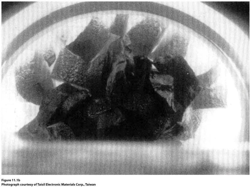
After three high-temperature chemical reactions, we obtain solid silicon, but this silicon is polycrystalline silicon.
What is polycrystalline silicon?
It’s like when we peel an orange, there are many segments of orange (polycrystalline orange), and the taste of different segments is different (crystal direction). We need to select the best-tasting segment and let it grow alone!
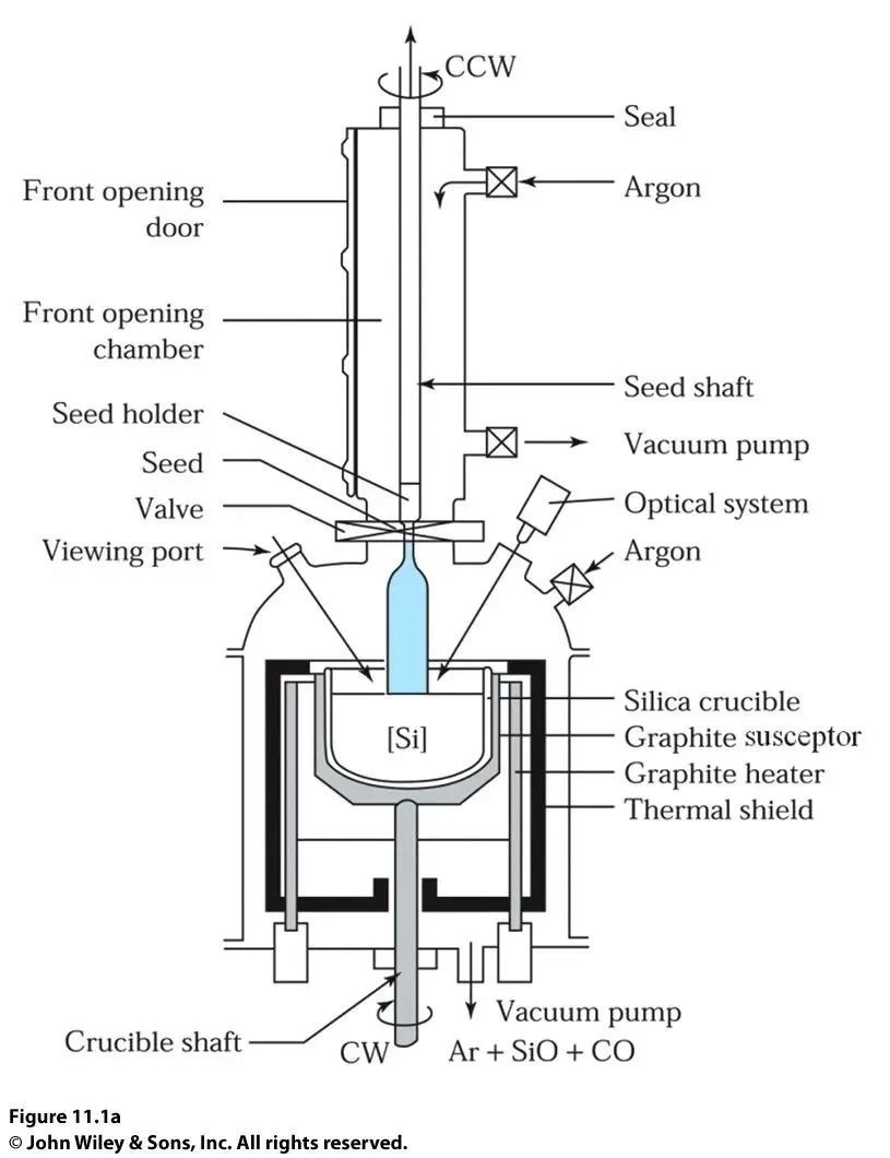
How to let a small single crystal grow alone?
Physicists are quite clever; they invented a method to grow single crystals called the Czochralski method, likely named after this scientist.
There is also an intuitive industry term called the pulling method!
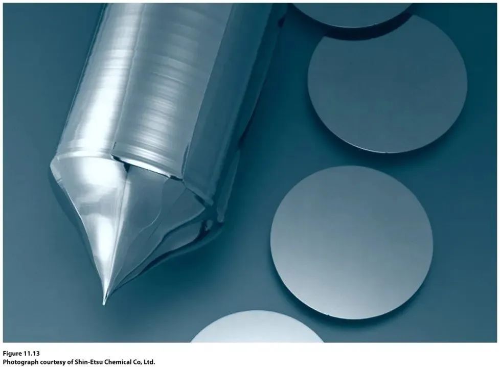
Because during the growth of single crystals, the small crystal is pulled upwards slowly. Let’s take a look at this device:
The blue rod in the image is single crystal silicon. During the pulling process, it rotates while being pulled upwards, and the crystal ingot produced by the pulling method is cylindrical.
The long crystal ingot is then cut into round disks using mechanical blades, becoming wafers.
This is how wafers are produced. Although we have obtained wafers, the electrochemical performance of single crystal silicon is still not good enough for direct use in chips, so engineers find ways to modify the electrochemical performance of single crystal silicon.
How to modify single crystal silicon?
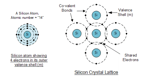
First, let’s take a closer look at silicon. In the periodic table, silicon is in the 14th position. Silicon atoms have 4 electrons in their outer shell, which share 4 pairs of electrons with 4 surrounding atoms; this structure of shared electron pairs is called covalent bonding.
Each electron pair forms a covalent bond, a part of knowledge learned in middle school chemistry.
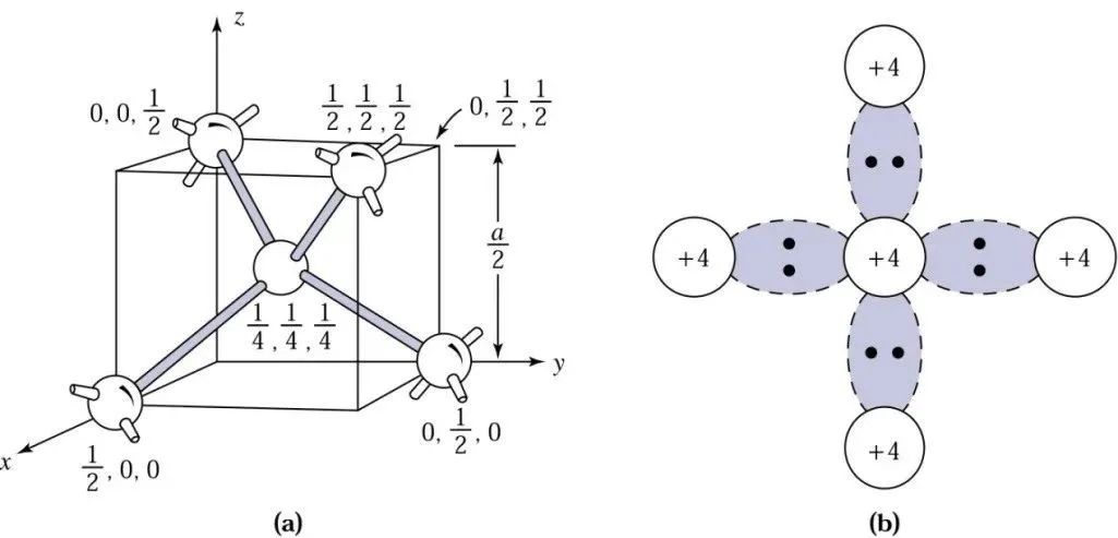
Let’s look at another image for a visual understanding:
The left image shows the crystal structure of single crystal silicon, which has a diamond crystal structure. The right image shows the situation of silicon atoms sharing electrons, where one silicon atom shares electrons with four silicon brothers.
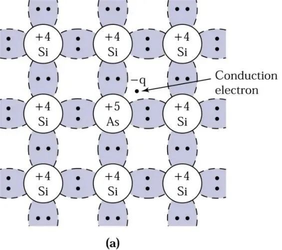
One day, a physicist thought, what if silicon doesn’t share electrons with silicon brothers but brings in other brothers? What would happen?
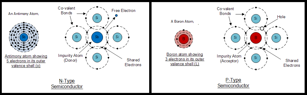
One day, the physicist brought arsenic into the group, and a miracle happened:
The arsenic brother has 5 electrons in its outer shell, where 4 electrons found partners with silicon, while one electron remained single. This electron became a free electron, roaming everywhere. Since electrons carry charge, it changed the conductivity of silicon.
At this point, the arsenic atom provided an additional electron to silicon, hence arsenic atoms are called donors.
With the increase of free electrons, silicon becomes an n-type semiconductor.
Why is it called n-type? In English, Negative represents negative, and the first letter of this word is N.
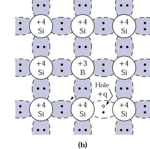
Similarly, physicists wondered, since we can bring in arsenic with extra electrons, can we also bring in boron, which has fewer electrons?
Since boron has only 3 electrons in its outer shell, one less than silicon, the originally 2 pairs of electrons in the covalent bond now become only one pair of electrons, creating one vacancy, which becomes a positively charged hole.
At this point, the silicon-based semiconductor is called a p-type semiconductor, and similarly, P comes from the first letter of the English word Positive (positive), while boron atoms are called acceptors.
It is precisely the different atoms added to single crystal silicon that form n-type and p-type semiconductors.
The following image shows the formation of p-type and n-type semiconductors after adding the elements tellurium (with 5 outer electrons) and boron (with 3 outer electrons).
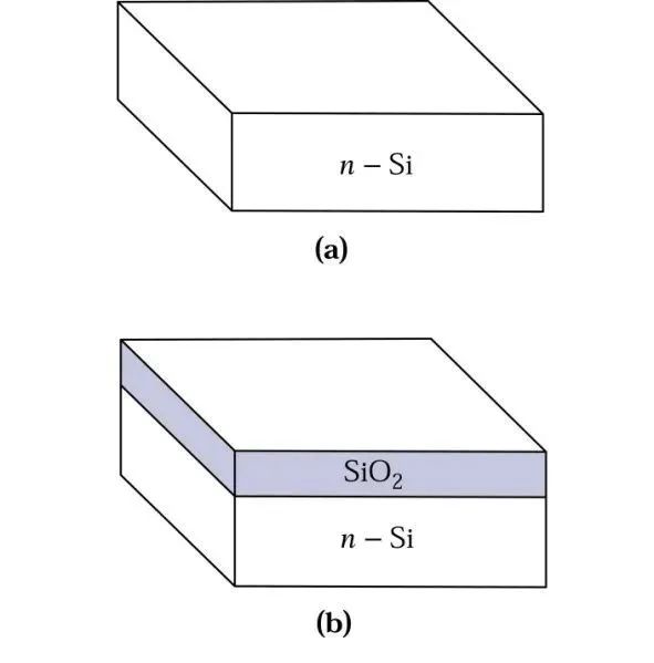
Once we have single crystal silicon, we can oxidize the surface to silicon dioxide. Silicon dioxide can serve as an insulator for many device structures or act as a barrier layer during the device fabrication process, such as defining the junction area in the manufacturing process of p-n junctions. Let’s take a look at a schematic diagram: (a) shows a silicon wafer without a cover layer, ready for oxidation, and (b) shows the upper surface of the oxidized wafer.
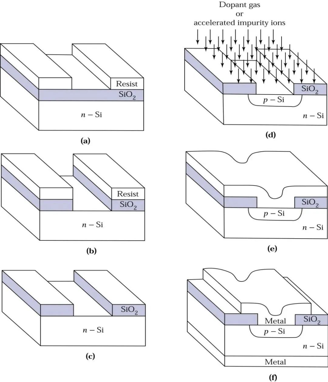
With the theoretical knowledge of p-type and n-type semiconductors, we can play with more complex designs, modifying the surface of silicon dioxide into the shapes we want, such as drawing a cat or a flower…
The method of modifying the surface of the wafer is called photolithography!
Isn’t photolithography done using high-end lithography machines?
Let’s first look at the principle of photolithography:
Using high-speed spin-coating equipment (spinner), a layer of UV-sensitive material, known as photoresist, is spun onto the surface of the wafer. After removing the wafer from the spinner, it is baked between 80ºC and 100ºC to drive off the solvent in the photoresist and harden it, enhancing the adhesion of the photoresist to the wafer. Next, a UV light source is used to expose the wafer through a patterned mask. Then, buffered hydrofluoric acid is used as an etchant to remove the silicon dioxide surface not protected by the photoresist. Finally, a chemical solvent or plasma oxidation system strips the photoresist. Let’s look at a schematic diagram:
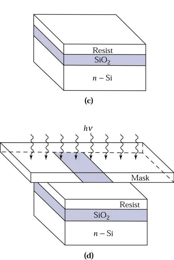 The description might be a bit complex; intuitively, it is somewhat like stamping: first, paint a model on a stone, and then carve according to the size of the model, which is basically the idea. Stamps have positive and negative engravings, and wafers can achieve the same based on the selection of photoresist, using positive and negative resists.
After photolithography, the silicon surface is exposed to the outside world. At this point, physicists introduce other elements into this silicon surface through various methods, known as ion implantation.
After injecting B or As ions, these ions change the traditional properties of silicon, resulting in a semiconductor known as extrinsic semiconductor. The junction formed by the contact of p-type and n-type semiconductors is called a p-n junction! After doping, we need to find a way to extract the properties of this semiconductor, so we metallize the surface of the semiconductor, completing ohmic contact and interconnect in the subsequent metallization steps. The metal film can be formed using PVD or CVD. With the completion of metallization, the p-n junction can work!
So, what exactly is the p-n junction that we often hear about?
(1) Principle of the PN Junction
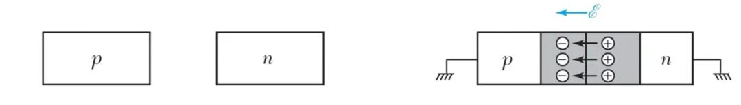
The left image shows a p-type semiconductor and an n-type semiconductor, which do not exhibit electrical properties when they exist independently.
When they are joined together, the holes from the p-type want to visit the n-type, and the electrons from the n-type also want to visit the p-type.
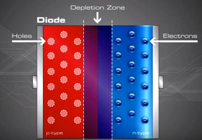
They move towards each other’s territory, and as they walk, they suddenly realize that electrons can fall into holes, and holes can completely accept electrons. In the area where they meet, there are no holes or electrons left (because they have recombined), and this region is called the depletion region.
Since there is a depletion region in the middle, electrons cannot move, and holes cannot move either.
What if we give these electrons a little push? What will happen?
How to push? Then apply an electric field to this p-n junction; with an electric field, there will be electron flow.
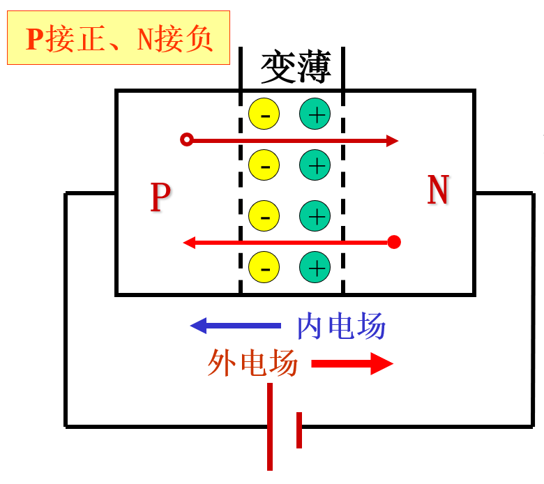
When people connect the p-type semiconductor to the positive terminal and the n-type semiconductor to the negative terminal, it looks like this:
Applying a positive voltage makes the potential of the p region higher than that of the n region, called forward voltage, or simply forward bias;
When the p-n junction is forward biased, it narrows, the forward current is large, and the forward resistance is small, putting the p-n junction in a conducting state.
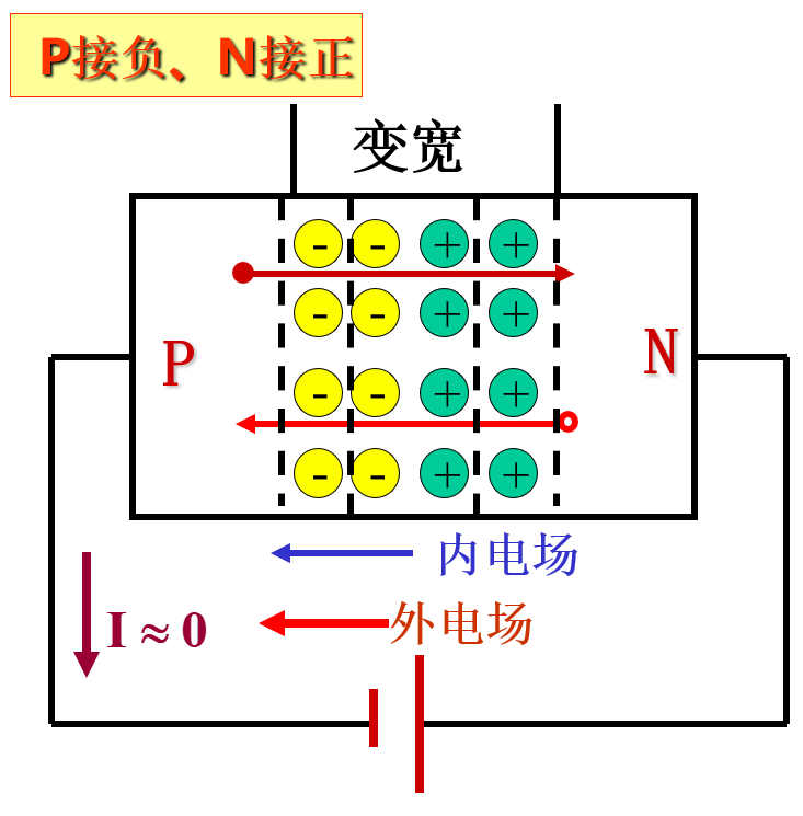
Someone proposed an idea: what if we reverse the positive and negative terminals connected to the p-n junction?
When the applied voltage makes the potential of the p region lower than that of the n region, it is called reverse voltage, or simply reverse bias;
When the p-n junction is reverse biased, it widens, the reverse current is small, and the reverse resistance is large, putting the p-n junction in a cutoff state.
By applying different directions of voltage to the p-n junction, we get:
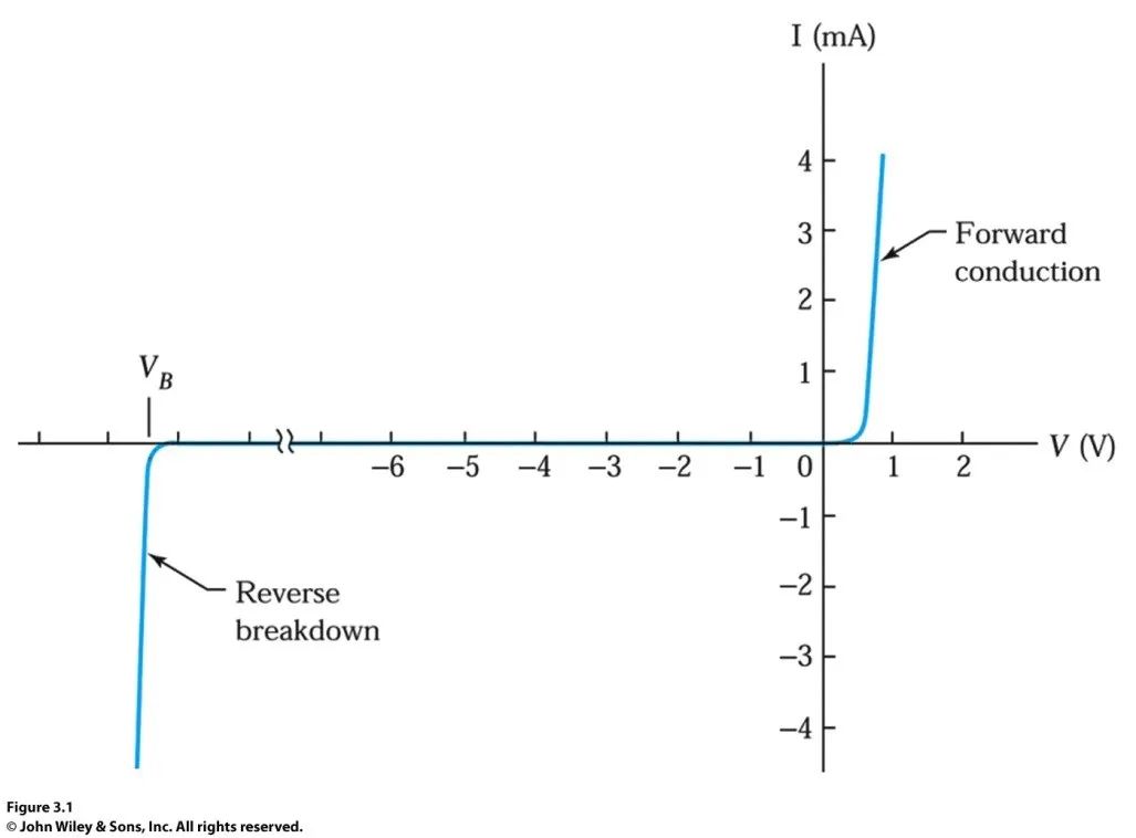
(1) When a positive voltage is applied to the p-n junction, it exhibits low resistance and has a large forward diffusion current, allowing the p-n junction to conduct.
(2) When a reverse voltage is applied to the p-n junction, it exhibits high resistance and has a very small reverse drift current, cutting off the p-n junction.
From this, we can conclude that the p-n junction has unidirectional conductivity.
Thus, the current-voltage curve of the p-n junction looks like this:
(2) Principle of the Diode
After scientists invented the p-n junction and discovered its characteristics, they began to enter the practical phase.
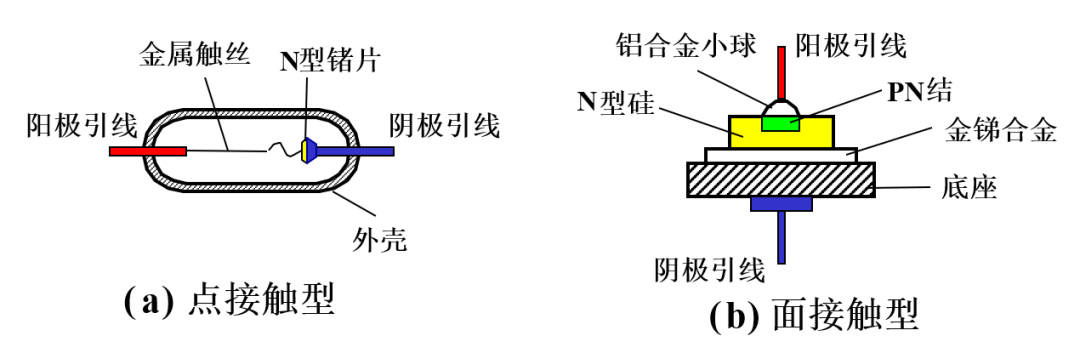
By adding a shell and leads to the p-n junction, it becomes a semiconductor diode.
The structure of the diode is shown in the following image:
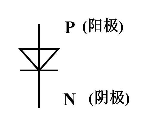
The diode symbol is also very common:
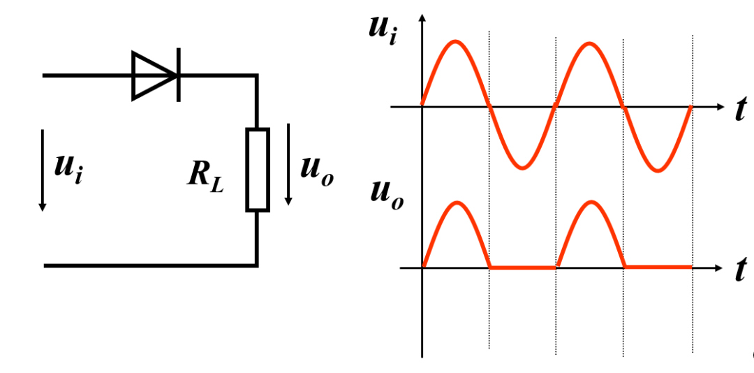
Based on the unidirectional conduction characteristics of diodes, they can be used for rectification, detection, clipping, clamping, switching, component protection, temperature compensation, etc.
For example, in a half-wave rectification circuit using a diode, the voltage can pass through in the forward direction but cannot pass in the reverse direction, thus leaving the forward half-wave voltage.
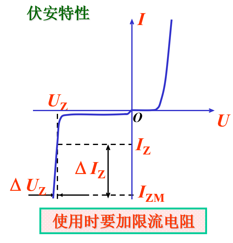
In addition to the function of forward bias, people found that reverse bias of diodes also has certain uses.
When a reverse voltage is applied to the diode during operation, it is called a voltage regulator. After reverse breakdown, the current changes significantly, but the voltage across it changes very little. Utilizing this characteristic, the voltage regulator can stabilize voltage in a circuit.
Therefore, we can conclude:
(1) When a forward voltage (forward bias, anode connected to positive, cathode connected to negative) is applied to the diode, it is in a forward conducting state, with low forward resistance and large forward current.
(2) When a reverse voltage (reverse bias, anode connected to negative, cathode connected to positive) is applied to the diode, it is in a reverse cutoff state, with high reverse resistance and very small reverse current.
(3) If the applied voltage exceeds the reverse breakdown voltage, the diode will break down and lose its unidirectional conductivity.
(4) The reverse current of the diode is influenced by temperature; the higher the temperature, the larger the reverse current.
(3) Principle of the Transistor
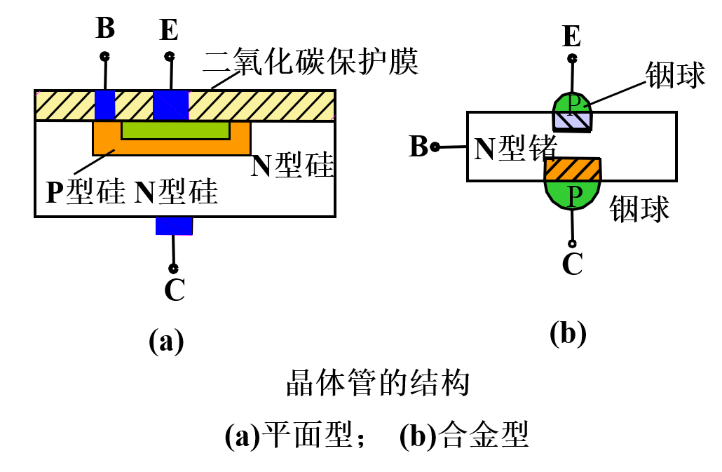
When p-type and n-type semiconductors are arranged together in a PNP or NPN formation, a transistor is formed. The structural diagram of a semiconductor transistor is shown below:
The three electrodes of the transistor are called the emitter, collector, and base.
If the transistor is made into a semiconductor device, its internal structure is shown in the following image:
Transistors are also known as bipolar junction transistors.
With the prototypes of diodes and transistors, all other semiconductor devices are based on the modification, upgrading, and optimization of diodes and transistors!
The p-n junction is the foundation of all semiconductor devices, just as rice and flour are the basis of food; flour can be made into buns, steamed buns, bread, noodles…
The description might be a bit complex; intuitively, it is somewhat like stamping: first, paint a model on a stone, and then carve according to the size of the model, which is basically the idea. Stamps have positive and negative engravings, and wafers can achieve the same based on the selection of photoresist, using positive and negative resists.
After photolithography, the silicon surface is exposed to the outside world. At this point, physicists introduce other elements into this silicon surface through various methods, known as ion implantation.
After injecting B or As ions, these ions change the traditional properties of silicon, resulting in a semiconductor known as extrinsic semiconductor. The junction formed by the contact of p-type and n-type semiconductors is called a p-n junction! After doping, we need to find a way to extract the properties of this semiconductor, so we metallize the surface of the semiconductor, completing ohmic contact and interconnect in the subsequent metallization steps. The metal film can be formed using PVD or CVD. With the completion of metallization, the p-n junction can work!
So, what exactly is the p-n junction that we often hear about?
(1) Principle of the PN Junction
The left image shows a p-type semiconductor and an n-type semiconductor, which do not exhibit electrical properties when they exist independently.
When they are joined together, the holes from the p-type want to visit the n-type, and the electrons from the n-type also want to visit the p-type.
They move towards each other’s territory, and as they walk, they suddenly realize that electrons can fall into holes, and holes can completely accept electrons. In the area where they meet, there are no holes or electrons left (because they have recombined), and this region is called the depletion region.
Since there is a depletion region in the middle, electrons cannot move, and holes cannot move either.
What if we give these electrons a little push? What will happen?
How to push? Then apply an electric field to this p-n junction; with an electric field, there will be electron flow.
When people connect the p-type semiconductor to the positive terminal and the n-type semiconductor to the negative terminal, it looks like this:
Applying a positive voltage makes the potential of the p region higher than that of the n region, called forward voltage, or simply forward bias;
When the p-n junction is forward biased, it narrows, the forward current is large, and the forward resistance is small, putting the p-n junction in a conducting state.
Someone proposed an idea: what if we reverse the positive and negative terminals connected to the p-n junction?
When the applied voltage makes the potential of the p region lower than that of the n region, it is called reverse voltage, or simply reverse bias;
When the p-n junction is reverse biased, it widens, the reverse current is small, and the reverse resistance is large, putting the p-n junction in a cutoff state.
By applying different directions of voltage to the p-n junction, we get:
(1) When a positive voltage is applied to the p-n junction, it exhibits low resistance and has a large forward diffusion current, allowing the p-n junction to conduct.
(2) When a reverse voltage is applied to the p-n junction, it exhibits high resistance and has a very small reverse drift current, cutting off the p-n junction.
From this, we can conclude that the p-n junction has unidirectional conductivity.
Thus, the current-voltage curve of the p-n junction looks like this:
(2) Principle of the Diode
After scientists invented the p-n junction and discovered its characteristics, they began to enter the practical phase.
By adding a shell and leads to the p-n junction, it becomes a semiconductor diode.
The structure of the diode is shown in the following image:
The diode symbol is also very common:
Based on the unidirectional conduction characteristics of diodes, they can be used for rectification, detection, clipping, clamping, switching, component protection, temperature compensation, etc.
For example, in a half-wave rectification circuit using a diode, the voltage can pass through in the forward direction but cannot pass in the reverse direction, thus leaving the forward half-wave voltage.
In addition to the function of forward bias, people found that reverse bias of diodes also has certain uses.
When a reverse voltage is applied to the diode during operation, it is called a voltage regulator. After reverse breakdown, the current changes significantly, but the voltage across it changes very little. Utilizing this characteristic, the voltage regulator can stabilize voltage in a circuit.
Therefore, we can conclude:
(1) When a forward voltage (forward bias, anode connected to positive, cathode connected to negative) is applied to the diode, it is in a forward conducting state, with low forward resistance and large forward current.
(2) When a reverse voltage (reverse bias, anode connected to negative, cathode connected to positive) is applied to the diode, it is in a reverse cutoff state, with high reverse resistance and very small reverse current.
(3) If the applied voltage exceeds the reverse breakdown voltage, the diode will break down and lose its unidirectional conductivity.
(4) The reverse current of the diode is influenced by temperature; the higher the temperature, the larger the reverse current.
(3) Principle of the Transistor
When p-type and n-type semiconductors are arranged together in a PNP or NPN formation, a transistor is formed. The structural diagram of a semiconductor transistor is shown below:
The three electrodes of the transistor are called the emitter, collector, and base.
If the transistor is made into a semiconductor device, its internal structure is shown in the following image:
Transistors are also known as bipolar junction transistors.
With the prototypes of diodes and transistors, all other semiconductor devices are based on the modification, upgrading, and optimization of diodes and transistors!
The p-n junction is the foundation of all semiconductor devices, just as rice and flour are the basis of food; flour can be made into buns, steamed buns, bread, noodles…
END
Reprinted content represents only the author’s views
It does not represent the position of the Semiconductor Institute of the Chinese Academy of Sciences
Editor: Schrödinger’s Cat
Responsible Editor: Three Dollar Fish
Submission Email: [email protected]
1. The Semiconductor Institute has made progress in bionic covering neuron models and learning methods
2. The Semiconductor Institute has made significant progress in inverted structure perovskite solar cells
3. Why is copper used as interconnect metal in chips?
4. What exactly is the 7nm in chips?
5. Silicon-based integrated optical quantum chip technology
6. How anomalous is the quantum anomalous Hall effect? It may bring about the next information technology revolution!