Warm reminder: The article is about 3400 words long and will take about 10 minutes to read. You will definitely gain insights after reading it. If you want to learn more professional knowledge and industry information, you can join my knowledge community and grow continuously with me. When it comes to flexible printed circuit boards (FPCA), most people are very familiar with it. As one of the core components in display modules, FPCA plays a “crucial” role in the entire display module. If we compare the display module to a “human”, FPCA is like the “blood vessels” in the body, providing the “pipeline” for the “blood” to flow within.In the entire manufacturing process of FPCA, if there are no issues, that’s fine; however, once a problem occurs, it is basically not a small issue, belonging to the nature of 0 and 1.Given the importance of FPCA in the display industry, most brand clients will give FPCA “special care”. During project development, brand clients will require FPCA or module manufacturers to provide FPCA samples, which will then undergo a comprehensive “dissection” to determine whether they meet usage requirements.Here, the “dissection” of FPCA is defined by a specific term in the industry, namely:Electronic componentsDestructive Physical Analysis (DPA) is an analysis method used to evaluate the internal structure, material composition, process quality, and reliability of electronic components (such as integrated circuits, semiconductor devices, resistors, capacitors, etc.).So, during the DPA slicing process of flexible printed circuit boards (FPCA), what positions should be sliced? What are the key focus points?Today’s article will mainly focus on the DPA slicing process, starting from the relevant thickness and dimensions of FPCA, and the appearance and morphology of FPCA, to provide readers with a comprehensive understanding of the focus points in FPCA DPA slicing.01 Testing of FPCA Thickness and DimensionsFlexible printed circuit boards (FPCA) are made from many materials through multiple processing steps, and different materials and process requirements have a significant impact on the performance of FPCA. In FPCA DPA slicing, there are many important thicknesses and dimensions that need to be tested.① Thickness of each layer of FPCA materialsThe main materials that make up FPCA include substrates (with copper foil), cover films (with thermosetting adhesive), thermosetting green oil, electromagnetic shielding film (EMI), components, BTB connectors, PI/steel sheet reinforcements, and encapsulation adhesives. We will focus on substrates, copper foil, cover films, and thermosetting green oil.
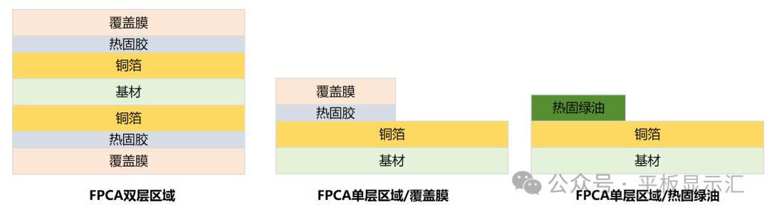 Illustration of material layering in different areas of FPCAa. Substrate: Mainly divided into adhesive substrates and non-adhesive substrates; a substrate with copper foil on one side is generally referred to as a single-sided board, while a substrate with copper foil on both sides is referred to as a double-sided board.In display modules, the mainstream substrate thickness used for FPCA is generally 20um and 25um.b. Copper foil: Copper foil is mainly divided into electrolytic copper foil and rolled copper foil. We have detailed this in previous articles.【Technical Insights】Understand the manufacturing processes and key performance of rolled copper foil and electrolytic copper foil in one articleIn display modules, the mainstream thickness of copper foil used in FPCA is generally 12um (excluding surface copper thickness), which is 1/3Oz. Generally, non-adhesive electrolytic copper is used. Here, “non-adhesive” refers to the substrate not having adhesive.Fun Fact: 1Oz (ounce) = 36umc. Cover film: The cover film mainly consists of two parts, namely PI (polyimide) and thermosetting adhesive. In display modules, the thickness of PI used in FPCA is generally 0.5mil, which is 12.5um; the thickness of thermosetting adhesive is generally 15um.Fun Fact: 1mil = 25.4umd. Thermosetting green oil: Thermosetting green oil has good bending properties after curing and is generally printed on the single layer of FPCA that needs to be bent. In display modules, the thickness of thermosetting green oil in the bending area of FPCA is generally controlled at 15±5um.Now that we understand the main material composition and thickness of FPCA, DPA slicing needs to test whether the thickness of each layer meets design and selection requirements to ensure the key performance of FPCA.
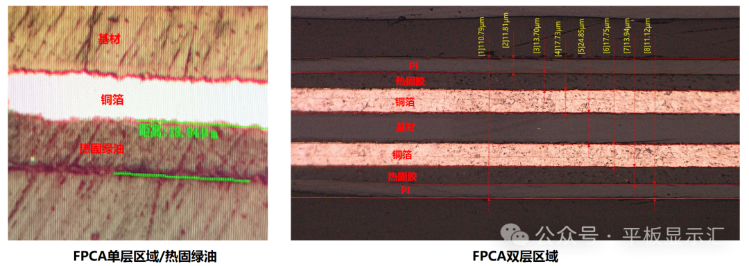 Illustration of DPA slicing thickness testing in different areas of FPCA② Testing of through-hole diameter in FPCA In double-sided FPCA, through-holes mainly serve to connect the top layer circuits and bottom layer circuits. The size of the through-hole diameter will affect the drilling yield and efficiency of FPCA manufacturers, as well as the electrical and mechanical performance of FPCA, line density, space utilization, and current carrying capacity, among other aspects.In display modules, the mainstream through-hole diameters for FPCA are generally 0.15mm and 0.1mm, and DPA slicing needs to test whether the through-hole diameter meets the requirements of the Gerber data.
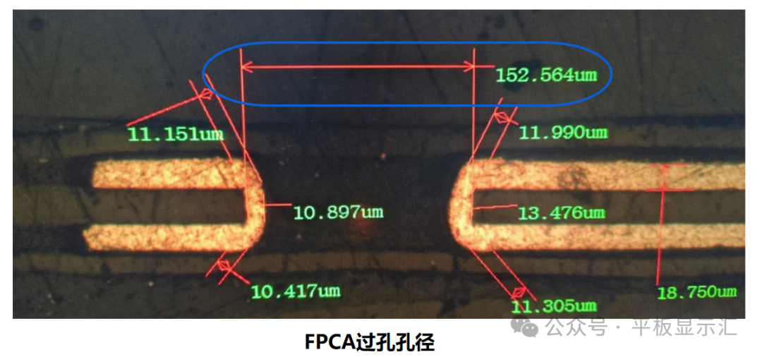 Illustration of DPA slicing testing for through-hole diameter in FPCA③ Testing of copper thickness in through-holes of FPCA If FPCA only has through-holes, it cannot achieve the connection between the top layer circuits and bottom layer circuits. It is necessary to perform black hole treatment at the through-hole first, and then copper plating, ultimately forming a layer of electroplated copper on the hole wall, known as hole copper.Control of hole copper thickness is very critical; if the hole copper thickness is too thin, it will affect the electrical performance of FPCA, such as increasing the DC resistance at the through-hole; on the other hand, it will affect the mechanical reliability of FPCA, as under thermal stress, thin hole copper is prone to the risk of hole wall fracture.In display modules, the copper thickness of through-holes in FPCA is generally controlled at ≥8~10um, and DPA slicing needs to test whether the hole copper meets design requirements.
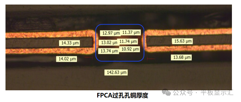 Illustration of DPA slicing testing for copper thickness in through-holes of FPCA④ Testing of gold-nickel layer thickness in FPCA The thickness of the gold-nickel layer in FPCA should be well understood; copper foil is very prone to oxidation when exposed to air for a long time, which can lead to reduced bonding strength, increased contact resistance, and affect the integrity of signal transmission. Therefore, it is necessary to perform nickel-gold treatment on the surface of copper foil to prevent oxidation, ultimately improving the environmental reliability of FPCA.In display modules, if there are salt spray testing requirements, the thickness of the gold-nickel layer on the surface of FPCA copper foil is generally controlled at a nickel layer thickness of 2.5~6um and a gold layer thickness of 0.05~0.11um; if there are no salt spray requirements, based on cost considerations, the thickness of the gold-nickel layer can be appropriately reduced.FPCA DPA slicing is one of the methods to test the thickness of the gold-nickel layer; since the thickness of the gold layer is too thin to be tested, the main focus is on testing the nickel layer thickness. Currently, the mainstream method in the industry is to use X-RAY to test the thickness of the gold-nickel layer.
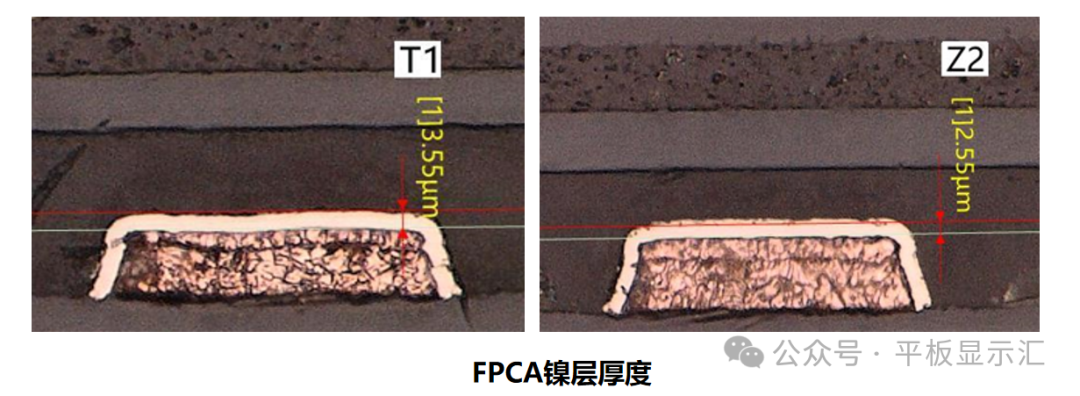 Illustration of DPA slicing testing for nickel layer thickness in FPCA⑤ Testing of etching factor in FPCA In the process of making FPCA circuits, the etching factor is a very critical control indicator; the etching factor can lead to deviations in line width and spacing, uneven copper foil thickness after etching, incomplete etching causing micro-short circuits, excessive line roughness, and burrs at the edges leading to impedance consistency deviations, among other issues.In display modules, the etching factor (etching rate) of FPCA is generally controlled at ≥4.0; the etching factor is mainly derived from the calculation of copper foil thickness, bottom line width, and top line width.
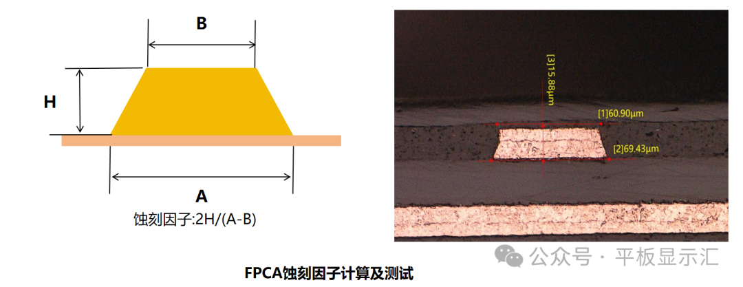 Illustration of etching factor calculation and DPA slicing testing in FPCA⑥ Testing of IMC layer thickness in FPCA When talking about the IMC layer in FPCA, most people may be unfamiliar; the IMC layer refers to intermetallic compounds, with the full English name:Intermetallic Compound. The IMC layer generally refers to compounds formed by the reaction of two or more metals under welding or high-temperature conditions. In FPCA, common IMC layers include: Cu-Sn IMC layer and Ni-Sn IMC layer. In display modules, the thickness of the IMC layer in FPCA is generally controlled within the range of 0.2~3um; the IMC layer can enhance the strength of solder joints, such as improving the thrust of components and BTB connectors; however, if the IMC layer is too thick, the risk of brittle fracture will also increase.
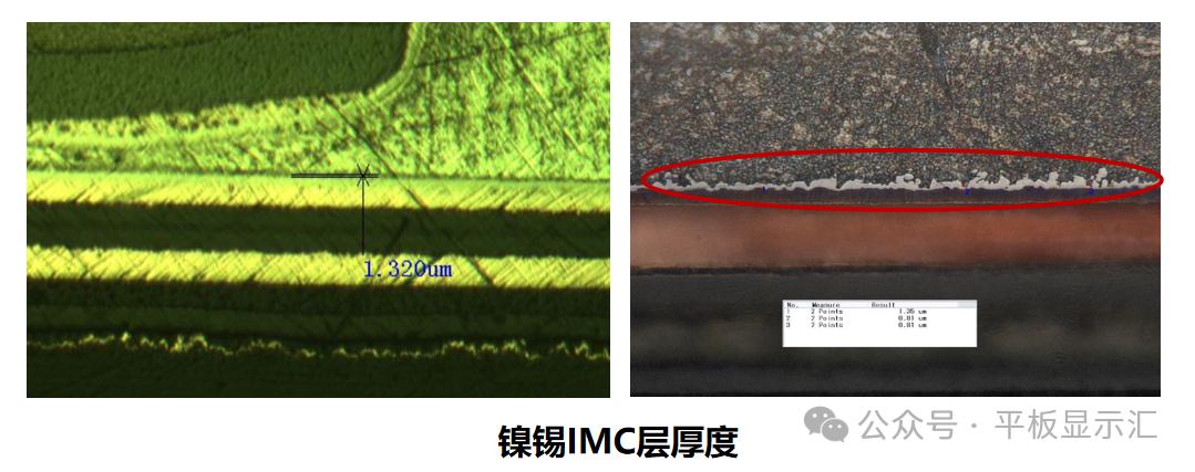 Illustration of DPA slicing testing for Ni-Sn IMC layer in FPCA⑦ Testing of adhesive for components on FPCA Many clients require adhesive to be applied around the pads of components on FPCA to reduce the risk of peeling or loosening during bending. This enhances the peeling strength and bending performance of the components. If the thickness and width of the adhesive are not controlled, it can easily lead to interference issues between the component area and the overall machine casing during installation.In display modules, the adhesive height on components on FPCA should not exceed the height of the component itself, and the adhesive width should be controlled according to a maximum overflow specification of 0.6~0.8mm from the component body, and DPA slicing needs to test whether the adhesive meets the specification requirements.
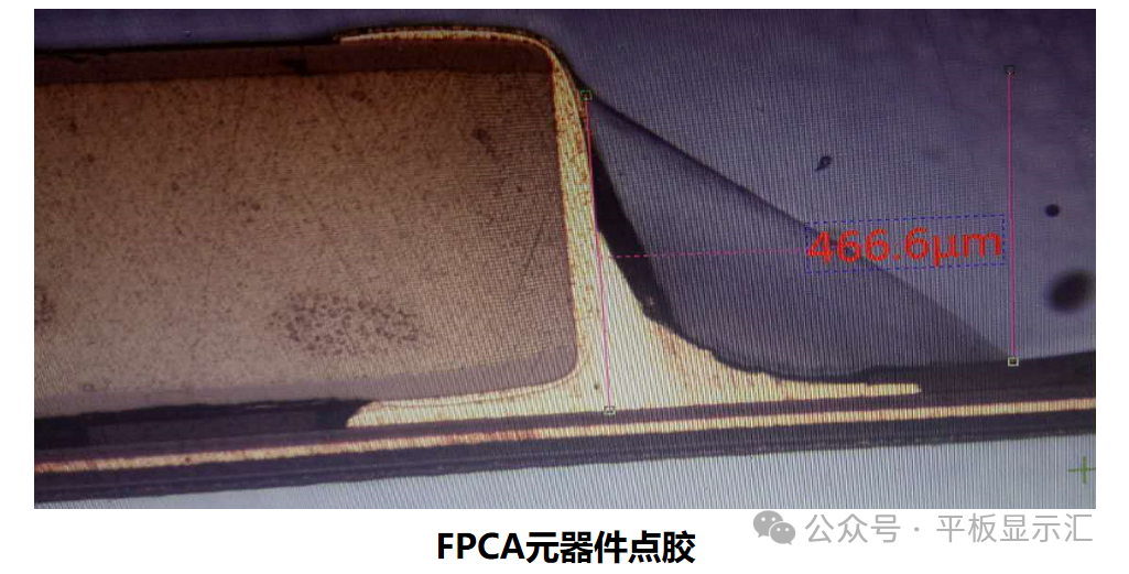 Illustration of adhesive application on components of FPCA02 Confirmation of FPCA Appearance and Morphology In addition to the thickness and dimension tests of FPCA mentioned in the first part, during DPA slicing of FPCA, it is also necessary to pay attention to the appearance and morphology that may affect the overall performance of FPCA, to avoid potential factors leading to failure in the display module later.① Confirmation of delamination in FPCA cover film and pads During the FPCA manufacturing process, there are many high-temperature steps, such as baking the FPC bare board before SMT, reflow soldering after SMT, and high-temperature curing after adhesive application. The high-temperature process generates thermal stress, which challenges the bonding strength between the cover film and copper foil, as well as between copper foil and substrate, and there is a risk of delamination. Therefore, during the FPCA DPA slicing process, it is necessary to closely observe and confirm whether there is any delamination between the various layers of materials, to proactively avoid the risk of failure in the display module.
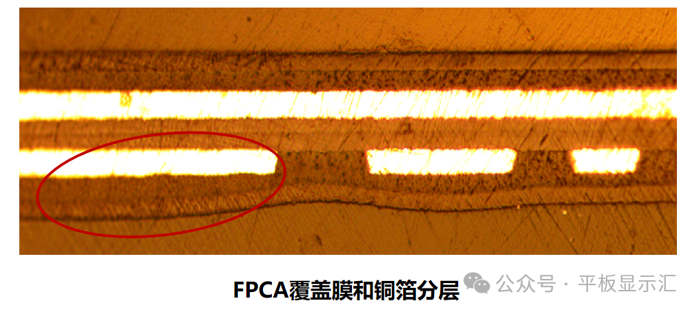 Illustration of delamination in FPCA DPA slicing cover film② Confirmation of solder cracking in FPCA component pads After the component placement on FPCA, there are still many handling processes; if the methods used during retrieval and packaging are unreasonable, it may impact the component pads, leading to solder cracking issues, which poses a hidden danger for the normal use of FPCA and may even directly cause defects. During the FPCA DPA slicing process, it is necessary to closely observe whether there are any solder cracking defects at the pads of components and BTB connectors.
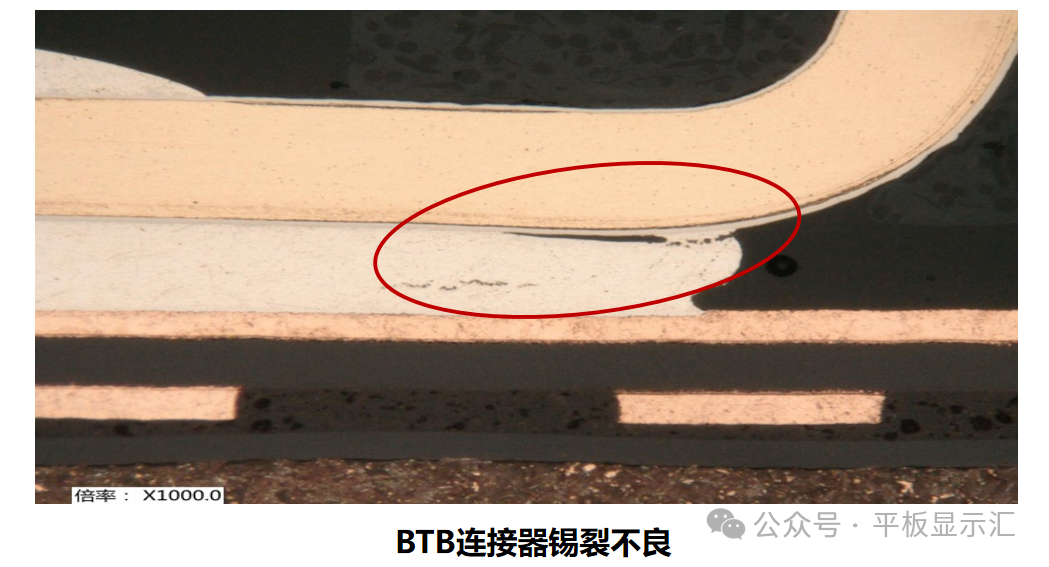 Illustration of solder cracking defects in FPCA DPA slicing BTB connectors③ Confirmation of nickel corrosion in FPCA Nickel corrosion is a common defect in FPCA, and the main causes of nickel corrosion are: due to the large lattice gaps in chemical nickel, during the displacement reaction, the gold complex ions in the plating solution attack along the nickel lattice interface, causing oxidation of the nickel surface, and excessive local reactions lead to the formation of nickel corrosion defects.
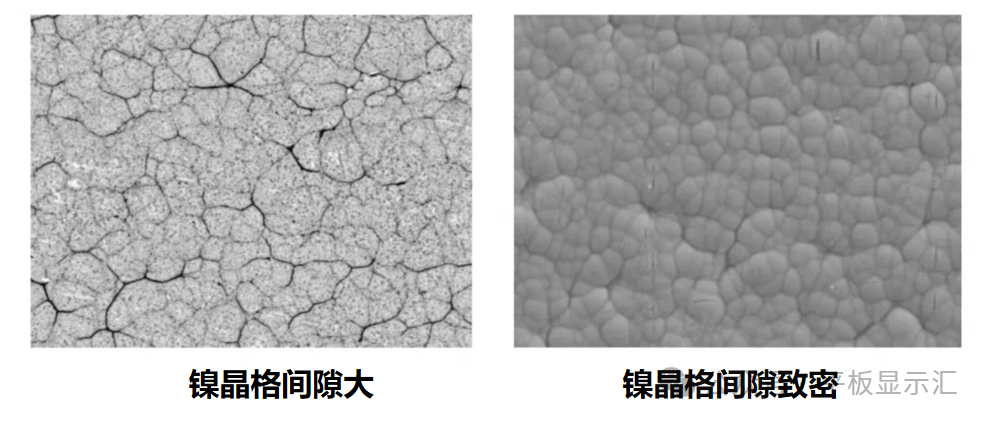 Illustration of different densities of nickel lattice surface morphology in FPCA Nickel corrosion can lead to reduced bonding performance of FPCA, decreased mechanical strength of pads, increased line resistance, and affected signal transmission. During the manufacturing process of FPCA, there are many influencing factors that can lead to nickel corrosion, such as nickel layer thickness, P content concentration, and the concentration of gold complex ions in the plating solution. Due to the length of the article, we will not elaborate on this.
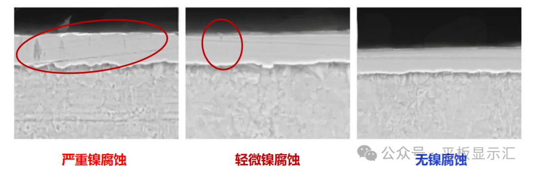 Illustration of different degrees of nickel corrosion in FPCA DPA slicingAlright, that concludes today’s sharing. This is acontent-rich public account, adhering to the principle of “speak without reservation”, follow me, and I hope it helps you.Author Profile:I am Uncommon, with over 10 years of experience in the display industry, having progressed from a technical novice to a technical director and product technology expert. I specialize in addressing various technical issues related to display products and hope to help everyone avoid the pitfalls I have encountered. Follow my public account, add me as a friend, and let me help you navigate the complexities of flat panel display technology. Remember to set it as a star mark so you can see articles as soon as they are published.
 Recommended previous articles:【Industry Insights】Discussing the Cost Influencing Factors of TFT-LCD Display Modules—CG Glass Cover Panel Edition【Practical Guide】Discussing the Mechanism of Rainbow Patterns in TFT-LCD and Improvement Strategies【Technical Insights】Understand the Manufacturing Processes and Key Performance of Rolled Copper Foil and Electrolytic Copper Foil in One Article【Technical Insights】Understand the Role, Structure, and Classification of Backlight Light Shielding Adhesives in One Article【Technical Insights】Understand the Dye Value of Glass Cover Ink and Its Influencing Factors in One Article【Technical Insights】Understand the Key Performance and Characterization Significance of Backlight Light Shielding Adhesives in One Article