
Author
Author
Stephen V.Chavez
Responsible for technical product marketing at Siemens EDA and serves as the chairman of the PCEA association.

The core of successfully delivering manufacturable PCB designs relies on a critical question: What should the design data output package include to best support manufacturing?
The answer is: It depends on the specific PCB design.
For specific categories of PCBs being designed for military/aerospace, space, medical, and commercial applications, many factors need to be considered. Other factors to consider are requirements and engineering objectives. More specifically, does the output file package contain all the necessary information required for manufacturing and assembly to meet engineering needs?
The industry best practice for transferring design output data to manufacturing is to establish close integration and collaboration with suppliers. The focus is to understand that suppliers are external stakeholders in the project. The key to achieving downstream success lies in optimizing the transition between engineering and manufacturing. This is rooted in the principles of Design For Manufacturing (DFM) and Manufacturing-Driven Design (MDD). A complete, correct, precise, intelligent, and collaborative data output package is not only good practice but is also critical for product quality, speed, and competitiveness.
The Purpose of PCB Design Output Packages
PCB design output packages are not just a set of files. They are the critical link between engineering design intent and manufacturing execution. The goal is to ensure that design data is correct through production, enabling manufacturing to be built with high yield, low cost, and high reliability. Its purposes are:
• Clearly communicate engineering design requirements
• Reduce the likelihood of errors or misunderstandings
• Simplify the manufacturing process
• Protect intellectual property
• Accelerate time to market
A well-crafted output file package, aligned with the strengths of manufacturing partners, can play a role in seamless product launches and high-cost delays. This is why close collaboration with suppliers needs to begin early in the project, often starting at project kickoff, with ongoing two-way communication throughout the design process.
Core Elements for Optimizing Output File Packages — Intelligence
Manufacturing File Formats: The Future of PCB Data
For decades, the Gerber file format has been the cornerstone of PCB manufacturing. This manufacturing output file format remains the primary file format required by most manufacturing suppliers. However, in today’s era of intelligent systems, new formats like ODB++ and IPC-2581 have advantages in functionality, integration, and reliability.
• ODB++: An ASCII-based compressed directory structure format. A single file package can provide complete data. Currently, nearly half of the industry companies are using this format.
• IPC-2581: An open, XML-based format that contains all necessary design data in a single file, making it ideal for IP control and intelligent data exchange.
While Gerber RS-274X is still widely accepted, it is limited by its lack of intelligence and reliance on auxiliary files. On the other hand, intelligent formats reduce manual interpretation, minimize errors, and support advanced DFM analysis.
No matter what manufacturing output file format is generated, the best approach is to work directly with the engineering design team of the manufacturer, not just sales personnel, to determine the preferred format. This ensures communication of requirements between design and manufacturing and reduces the risk of miscommunication. Early and frequent two-way communication is key.
Manufacturing and Assembly Drawings
Correct and precise drawings are crucial for explaining how to produce circuit boards. These drawings are based on industry standard IPC-D-325A. They may vary due to design and assembly, but should at least include:
• Descriptions of applicable reference information, such as relevant IPC standards, materials, solder mask, silkscreen, testability information, impedance requirements, conductor definitions (trace/spacing) information, and file naming conventions
• Detailed information about layers, board thickness, copper thickness, process conditions, design concepts, and drilling tables (TH and HDI details)
• Tolerances (IPC product grades), surface coating specifications, testing requirements, markings, pad sizes (if allowed), assembly multi-array, and handling requirements
• Component types, placement and orientation identification, polarity, reference designators, special mounting and installation instructions, automatic test equipment, electrical test requirements, and fixtures
• Process technical specifications, conformal coating (if required), cleanliness requirements, mechanical hardware, hardware torque requirements, solder joint specifications, labels, and soldering, including solder paste
It is crucial to clearly indicate the IPC level (e.g., Level 2 or 3) to set expectations for inspection and quality levels.
The IPC standard tree (Figure 1) is a good reference for determining which specific IPC standards apply at various stages of the entire production process.
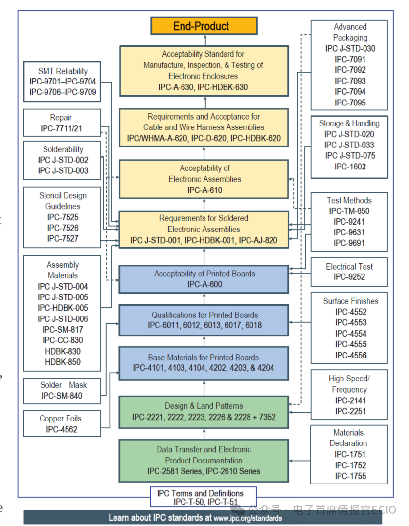
Figure 1: The IPC standards contain all the information needed from the start to the end of the production process. (Source: IPC Printed Board Component Production Checklist)
Comprehensive Bill of Materials (BOM)
The BOM should go beyond a parts list. It must have supply chain awareness, considering factors such as component availability, lifecycle status, potential obsolescence, and alternatives. By integrating supply chain intelligence at the design stage, known as supply chain resilient design, engineers can avoid costly late-stage redesigns or PCB redesigns.
3D CAD Models and Prototypes
3D models and prototypes support both virtual (also known as digital twin) and physical validation of designs. With the rise of model-based systems engineering, using digital twins and simulations to ensure component fit, mechanical integration, and thermal management is becoming the industry standard.
Process Descriptions and Testing Requirements
Step-by-step manufacturing instructions provide clarity on processes such as soldering, placement operations, and reflow soldering curves. Equally important are quality control technical specifications, which should incorporate testing practices into the design early in the project, as this is more cost-effective than retrofitting testing strategies.
When completing very complex designs, nothing is more frustrating for designers than hearing, “I know we initially agreed there were no test point requirements, but now we’ve decided we need to go back and add test points.”
For safety reasons, this is something that people might want to communicate to designers via email, phone, or at least from a distance, as making the decision to add test points after the fact can be infuriating.

The above is an advertisement and is not related to the main content.
Benefits of Optimizing Output Packages
Investing in a robust design output package can provide measurable value:
• Reduced Manufacturing Costs: Minimizing rework, scrap, and labor
• Accelerated Time to Market: Fewer technical queries and faster prototype production cycles
• Higher Product Quality: Standardized documentation reduces variability and errors
• Scalability: Easy-to-manufacture designs can be effortlessly scaled up
• Sustainability: Less material waste and more efficient processes support greener operations
Bridging the Gap Between Engineering and Manufacturing
The core of DFM success is collaboration. Engineers must view manufacturers not just as suppliers but as important project stakeholders. When selecting output formats and document types, the goal should not only consider compatibility but also the efficiency of both parties. Engineering design must be integrated with manufacturing considerations at the design stage, and efforts should be made to set up manufacturing for downstream success. This synergy can optimize manufacturing workflows, improve traceability, enhance component sourcing, and ultimately lead to more robust and profitable products.
Final Thoughts
A single file type or checklist does not define the best PCB design output package. It is the result of a continuous two-way communication and strategic collaboration process that combines intelligent data formats, comprehensive documentation, and a deep understanding of design and manufacturing constraints. By adopting modern DFM principles and moving beyond traditional output methods, engineering design teams can not only improve product quality and production speed but also build stronger and smarter connections with manufacturing partners.
END


The above are electronic chief information officer partners(partial)
Order does not imply priority