Design and Implementation of an Indoor Visible Light Communication System Based on FPGAWang Yifan, Wei Tongcheng, Zhang Bozhen, Zhang Yingxiang, Du YongXinjiang Normal University, College of Physics and Electronic Engineering, Key Laboratory of Luminescent Minerals and Optical Functional Materials
Reference Link
Wang Yifan, Wei Tongcheng, Zhang Bozhen, et al. Design and Implementation of an Indoor Visible Light Communication System Based on FPGA [J]. Journal of Xinjiang Normal University (Natural Science Edition), 2024, 43 (03): 21-30. DOI:10.14100/j.cnki.1008-9659.20240407.001.
Abstract
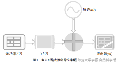
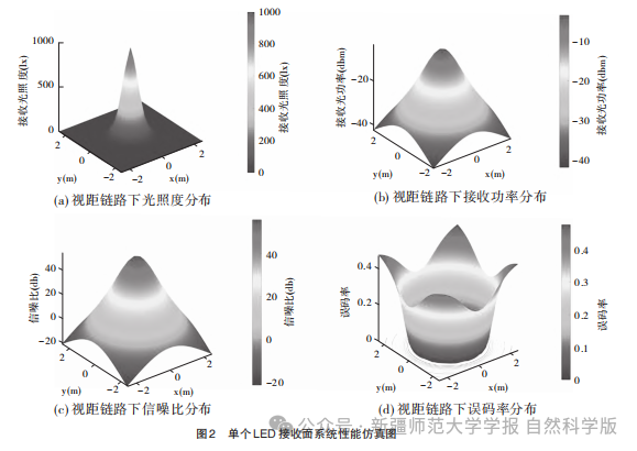
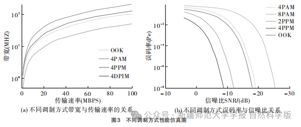
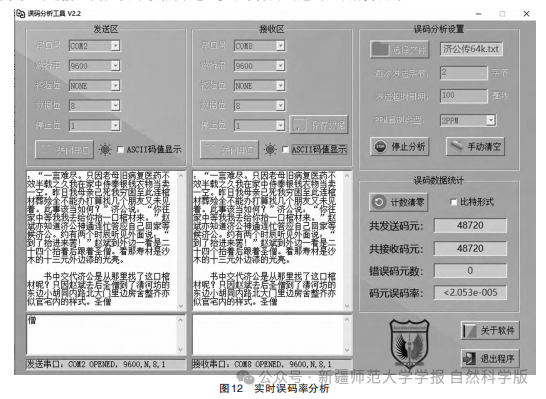
Visible Light Communication (VLC) has advantages such as high communication speed, environmental friendliness, high security, and no need for spectrum licensing, making it a current research hotspot. To address the complexity of VLC system design and the short communication distance, this paper adds a secondary amplification circuit at the receiving end to further improve the system’s anti-interference capability. It also studies the channel model of the indoor VLC system and conducts simulation analysis of illumination intensity, received power, signal-to-noise ratio, and bit error rate in indoor spaces using high-brightness light-emitting diodes. The analysis includes the noise resistance performance and bandwidth utilization of different modulation methods. The digital signal processor FPGA (Field Programmable Gate Array) is used as the control chip for the optical communication system, designing an indoor VLC system based on 2PPM (Pulse-Phase Modulation). An experimental platform was built to verify the system’s communication performance, achieving a bit error rate of less than 1×10⁻⁵ at a communication distance of 3.5m. The experimental results indicate that this communication system has low bit error rate and simple structure, meeting the requirements for high-performance indoor VLC systems.
Highlights
Field Programmable Gate Array
Pulse Position Modulation
Indoor Visible Light Communication
Secondary Amplification Circuit
Figures and Tables
Conclusion
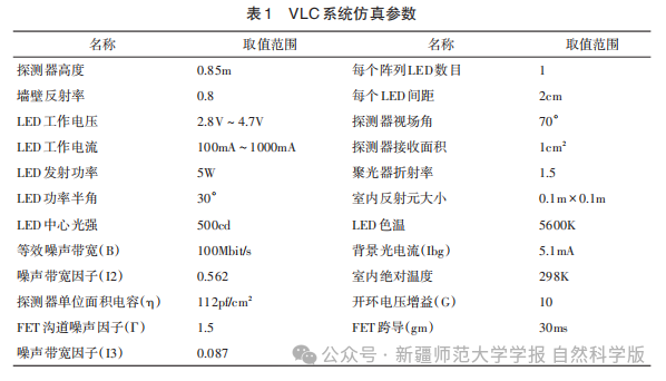
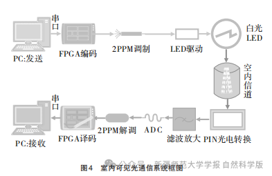
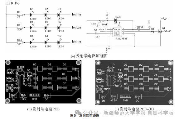
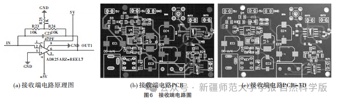
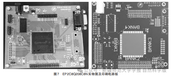
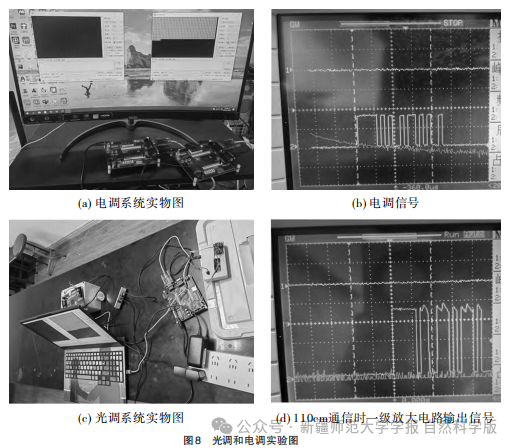
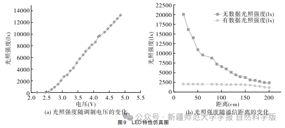
This article designs and implements an indoor visible light communication system based on 2PPM modulation, with an experimental communication distance set at 3.5m and a maximum data rate of 1Mbps. The hardware part of this experiment selects the EP2C8Q208C8N digital signal processor as the core processing chip, utilizing LED driving, ADC, and photodetectors to achieve reliable indoor visible light communication. For a single high-brightness LED, this experiment simulates the illumination intensity, received optical power, signal-to-noise ratio, and bit error rate of the indoor visible light communication system. The simulation results indicate that a single high-brightness LED can achieve reliable communication, but it cannot meet the lighting needs of an entire room. After multiple practical tests, the added secondary amplification circuit can improve the system’s reliability and reduce the bit error rate. This system has advantages such as simple structure, stable reliability, and low bit error rate, demonstrating certain engineering application value.
Source | Journal of Xinjiang Normal University (Natural Science Edition), 2024, Issue 3
Editor | Zhao Siliang
Deputy Editor | Liu Juan

Submission Email
↙ Click “Read the Original” for more exciting content